
HOWTO: Use STM32 SPI half duplex mode
HOWTO: Use STM32 SPI half duplex mode
I’ve got my hands onto some STM32F030F4P6 ARM-Cortex M0 processors.
Though touted as “32 cents 32-bit micro”, it is not that inexpensive from DigiKey in one-off quantity ($1.45).
However it is still cheaper than ATmegas and offers 3 times the performance.
The chip comes in 20-pin TSSOP package.
Limited pins require much more thoughts when assigning pin function.
For example, using 3-pin half-duplex SPI instead of 4-pin full-duplex SPI saves me 1 very precious GPIO pin.
It should be noted that not all SPI slave devices support half duplex mode,
and most devices will not mention half-duplex mode in the datasheets.
Generally, a SPI slave device supports half duplex SPI mode if:
- The device’s MISO (or DOUT) pin uses open-drain output.
- This is usually true because open-drain allows multiple SPI slaves to share the same MISO line.
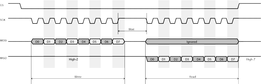
- In the communication protocol, the slave device always waits for the master to send fixed number of bytes (commands) from MOSI,
- then returns a fixed number of bytes to MISO.
- Some devices which transmit and receive data simultaneously cannot be used in half-duplex mode.
- The slave ignores whatever appears on the MOSI pin when transmitting data to the master.
- This is usually not mentioned in the datasheet.
- However, if the slave device mandates a CS or STROBE signal to be asserted at the beginning of each data exchange,
- we can usually assume this is true.
- Reason being that the slave device is using CS to reset its internal state
- rather than always listening and parsing command byte(s) from the master.
Half-duplex wiring of STM32 SPI is as follows:
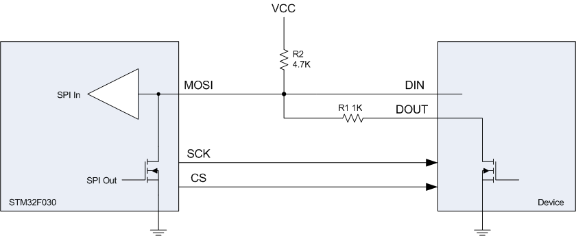
In particular, MOSI and SCK are configured as “Alternate Function” mode.
Hardware CS (NSS) management must be disabled and user shall manually control CS using GPIO output.
R2 is pull-up resistor as required by SPI.
R1 works as protection resistor in case STM32 MOSI pin somehow enters into push-pull output mode.
The SPI setup code is as follows:
void SPI_Configure()
{
    SPI_InitTypeDef SPI_InitStructure;
    // Enable SPI1 clock
    RCC_APB2PeriphClockCmd(RCC_APB2Periph_SPI1, ENABLE);
    // SPI1 configuration
    SPI_InitStructure.SPI_Direction = SPI_Direction_1Line_Tx; // Initially Tx
    SPI_InitStructure.SPI_Mode = SPI_Mode_Master;
    SPI_InitStructure.SPI_DataSize = SPI_DataSize_8b;
    SPI_InitStructure.SPI_CPOL = SPI_CPOL_High; // Clock steady high
    SPI_InitStructure.SPI_CPHA = SPI_CPHA_2Edge; // Data write on rising (second) edge
    SPI_InitStructure.SPI_NSS = SPI_NSS_Soft;
    SPI_InitStructure.SPI_BaudRatePrescaler = SPI_BaudRatePrescaler_64;
    SPI_InitStructure.SPI_FirstBit = SPI_FirstBit_LSB;
    SPI_InitStructure.SPI_CRCPolynomial = 7;
    SPI_Init(SPI1, &SPI_InitStructure);
    SPI_RxFIFOThresholdConfig(SPI1, SPI_RxFIFOThreshold_QF);
    SPI_Cmd(SPI1, ENABLE);
}
Line 7 sets the SPI peripheral to half-dulex transmission mode.
Line 17 sets the SPI FIFO buffer threshold to quarter full.
This is new in STM32F0 with 4-byte SPI FIFO buffer.
SPI_RxFIFOThreshold_QF meaning that the SPI_I2S_FLAG_RXNE flag will be set as soon as 1 byte
(quarter buffer) is shifted into receiving FIFO.
SPI master sending data to slave is as simple as:
void send_byte(uint8_t val)
{
    GPIO_ResetBits(GPIOA, GPIO_Pin_4); // CS low
    while (SPI_I2S_GetFlagStatus(SPI1, SPI_I2S_FLAG_TXE) == RESET); //wait buffer empty
    SPI_SendData8(SPI1, val);
    while (SPI_I2S_GetFlagStatus(SPI1, SPI_I2S_FLAG_BSY) == SET); //wait finish sending
    GPIO_SetBits(GPIOA, GPIO_Pin_4); // CS high
}
The following code demonstrates master sends 1 byte command to slave and reads 1 byte back.
 1 uint8_t send_and_read_byte(uint8_t cmd)
 2 {
 3     uint8_t result;
 4     GPIO_ResetBits(GPIOA, GPIO_Pin_4); // CS low
 5     while (SPI_I2S_GetFlagStatus(SPI1, SPI_I2S_FLAG_TXE) == RESET); //wait buffer empty
 6     SPI_SendData8(SPI1, cmd);
 7     while (SPI_I2S_GetFlagStatus(SPI1, SPI_I2S_FLAG_BSY) == SET); //wait finish sending
 8     // Read receiving FIFO until it is empty
 9     while (SPI_GetReceptionFIFOStatus(SPI1) != SPI_ReceptionFIFOStatus_Empty)
10         SPI_ReceiveData8(SPI1);
11     SPI_BiDirectionalLineConfig(SPI1, SPI_Direction_Rx);
12     while (!(SPI1->SR & SPI_I2S_FLAG_RXNE)) ; // wait data received
13     GPIO_SetBits(GPIOA, GPIO_Pin_4); // CS high
14     SPI1->CR1 |= SPI_Direction_Tx;  // Set Tx mode to stop Rx clock
15     result = SPI_ReceiveData8(SPI1);
16     return result;
17 }
Immediately after one byte is sent, the program empties all stale data in the FIFO (line 9, 10),
then sets SPI direction to receiving mode (line 11).
As soon as SPI enters into receiving mode, STM32 will continuously generate clock on SCK pin until receiving mode is disabled.
Along with the clock toggling, data are shifted from MOSI pin into receiving FIFO,
and SPI_I2S_FLAG_RXNE flag is set once 1 byte of data is received (line 12).
The program then disables CS (line 13, to disable slave output)
and switches SPI back to transmitting mode (line 14, to stop the clock).
These two steps must be executed fast enough before the next clock is sent out to prevent the slave device enter into any undefined state.
Timing is very critical here especially when SPI clock is high.
To receive multiple bytes from the slave, put line 9-15 into a loop but disable CS only after all data are read.
Important thing is to always disable receiving mode immediately after FIFO is quarter full,
and verify using a scope or logic analyser to ensure exact 8 clocks are send in-between each reading.

