
Programming Internal Flash Over the Serial Wire Debug <SWD> Interface -- EFM32
1 Debug Interface Overview
1.1 Serial Wire Debug
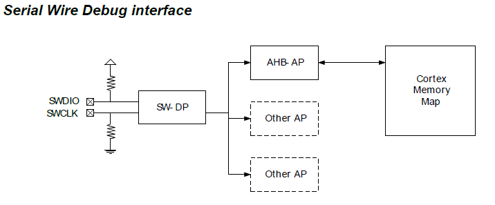
Serial Wire Debug (SWD) is a two-wire protocol for accessing the ARM debug interface.
It is part of the ARM Debug Interface Specification v5 and is an alternative to JTAG.
The physical layer of SWD consists of two lines:
• SWDIO: a bidirectional data line
• SWCLK: a clock driven by the host
Connecting to these pins allow an external device (such as a debug probe) to communicate directly
with the Serial Wire Debug Port (SW-DP).
The SW-DP in turn can access one or several Access Ports (APs) that give access to the rest of the system.
The important AP on the EFM32 is the AHB-AP which is a bus master on the internal AHB1 bus of the Cortex-M3.
In other words the AHB-AP can access the internal memory map of the core.
Since the internal flash, SRAM, debug components and peripherals all are memory mapped,
this AP can control the entire device including programming it.
Figure 1.1. Serial Wire Debug interface
Debug Pins
The EFM32 has three pins used for debugging.
Two of them are the SWDIO and SWCLK pins used by SWD.
The last pin is called Serial Wire Output (SWO) and is used for debugging output.
SWO is an asynchronous, one-directional protocol used by the internal debug components
in the core to output various debug information.
This pin is not required to program the device.
Out of reset both SWDIO and SWCLK are connected to SW-DP
and configured with a weak internal pullup and pull-down, respectively.
It is possible to disable both debug pins by configuring the GPIO_ROUTE register.
This can free up the pins to use them as GPIO. The SWO pin is initially disabled.
Note
Keep in mind that if the debug pins are disabled, a debugger will no longer be able to connect to the EFM32.
During development, it is therefore a good idea to make sure there is a delay
between reset and disabling the pins (typically a few seconds).
In that way the debugger has time to connect and halt the CPU before the pins are disabled.
If you have disabled the debug pins and are unable to connect to your device,
see Section 4.3 (p.13) for instructions on how to perform the debug unlock sequence.
When designing the debug header for a product it is common to also include the RESET pin
and one pin for sensing the supply voltage in addition to ground.
2 Serial Wire Programmers Model
This chapter describes the SWD protocol and how to communicate with the SW-DP and AHB-AP.
2.1 The SWD Protocol
In SWD terminology the host refers to the system controlling the debugger, i.e. the PC / debug probe.
The target is the system which is under debug, i.e. the EFM32.
SWCLK is a clock signal which is always driven by the host.
Both sides will drive the SWDIO line to send data.
A high value on SWDIO indicates a logical '1', a low value is a logical '0'.
The protocol specifies when each side will drive the SWDIO line.
Three different phases are specified.
Each transaction begins with the host sending a request.
The target answers with an acknowledge which is followed by a data phase.
Who controls the line during the data phase depends on the type of request issued by the host.
If the host issued a write request, the host will drive the line.
On a read request the target will drive the line to transmit data from the target to the host.
In all phases data is transmitted LSB (least significant bit) first.
The target will both sample and put data on the line on a rising clock edge.
Figure 2.1. SWD request
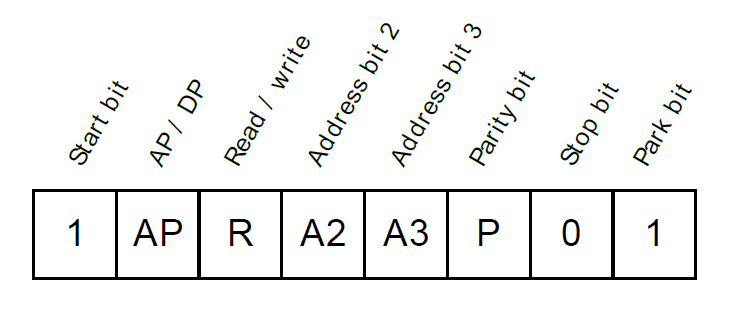
The request phase consists of 8 bits.
The meaning of each bit in the request is illustrated in Figure 2.1 (p.3) .
The start bit is always 1.
The next bit specifies whether the transaction is a DP (Debug Port) or AP (Access Port) transaction.
If this bit is zero, the transaction is a DP access.
Bit 2 is the read/write bit.
If this bit is 1 the transaction is a read access (from target to host).
Bit 3 and 4 are address bits A2 and A3.
These bits specifies which out of four registers are selected for the transaction.
Register selection is described in Section 2.2 (p. 5) .
Bit 5 is a parity bit. The parity bit is used by the target to verify the integrity of the request.
This bit should be 1 if bits 1-4 contains an odd number of 1's.
If the number of 1's are even, the parity bit should be zero.
Bit 6 is the stop bit. This bit is always zero.
Bit 7 is the park bit. This bit is always one.
The ack phase consist of three bits.
An OK response has the value 1.
Since values are put on the line LSB first
an OK response looks like a 1 followed by two 0's on the line.
Once the host has received an OK response the data phase can begin.
The data phase consists of 32 data bits (one word) followed by 1 parity bit.
The parity bit is calculated based on all the 32 data bits.
If the number of 1's in the data word is odd, the parity bit should be 1.
The host must continue to clock the interface for at least 8 cycles
after the data phase to make sure the transaction is clocked through the SW-DP.
This can be done either by:
- starting a new transaction
- inserting idle clock cycles, During idle clock cycles the SWDIO is driven low by the host
Figure 2.2. Successful Write Command (from [adi5])
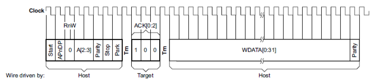
2.1.1 Turnaround Periods
Every time the SWDIO changes data direction, a one-cycle turnaround period is inserted which both sides should ignore.
This means there is always a turnaround period between the request and acknowledge.
On a write request, there is a turnaround period between acknowledge and the data phase.
On a read request there is a a turnaround after the data phase.
2.1.2 Initialization
Before using the SW-DP an initialization sequence must be performed to establish communication
and bring the SW-DP to a known state.
- 1. Perform a line resest
- 2. Send the JTAG-to-SWD switching sequence
- 3. Perform a line reset
- 4. Read the IDCODE register
A line reset is performed by clocking at least 50 cycles with the SWDIO line kept HIGH by the host.
The reason for the JTAG-to-SWD sequence is that the Debug Port implementation is actually a SWJ-DP.
SWJ-DP is a wrapper around both SW-DP and JTAG-DP, the JTAG counterpart to SWD.
The EFM32 does not include JTAG, but the switching sequence must still be performed
as the default state required by the SWJ-DP specification is JTAG.
The JTAG-to-SWD sequence is 0xE79E transmitted LSB first.
Figure 2.3. Read IDCODE SWD request
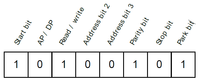
Figure Figure 2.3 (p. 4) shows the request command to read the IDCODE register.
After this request has been transmitted the target will reply with OK followed by the IDCODE value (and parity bit).
After this the debugger can use the SW-DP normally.
2.1.3 Errors
The SWD protocol specifies two other ACK responses than OK.
If the target responds with a WAIT response, the host must retry the operation later.
If the target responds with FAULT, an error has occured and one of the sticky bits in CTRL/STAT is set.
The host can check the sticky error bits to see what kind of error has occured.
It must clear the sticky bits before using any AP commands,
because the target will always respond with FAULT as long as one of the sticky error bits are set.
If the target sees a protocol error it will immediately stop driving the line,
i.e. it will not respond to any request.
If the host sees that the target does not drive the line
it must perform the initialization sequence again.
2.2 Serial Wire Debug Port Registers
Table 2.1. SW-DP registers
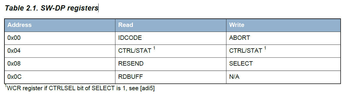
This section will give a brief overview over the SW-DP registers.
A full description of each register and the meaning of the individual bits can be found in [adi5].
Table 2.1 (p. 5) shows an overview over the SW-DP registers.
In the SWD request two address bits are given, ADDR[3:2].
Bits 1 and 0 of the address are always 0.
These bits select which register is accessed.
In addition the type of access (read or write) also affect which register is accessed.
As an example, say the transaction is a write access where address bits 2 and 3 are 0 and 1, respectively.
I.e. the address is 0b1000, or 0x8. This will choose the SELECT register.
The IDCODE register contains a identification value that identifies the SW-DP.
On the EFM32 devices with a Cortex-M3 or Cortex-M4 core this register should read 0x2BA01477.
For devices with a Cortex-M0+ core the register should read 0x0BC11477.
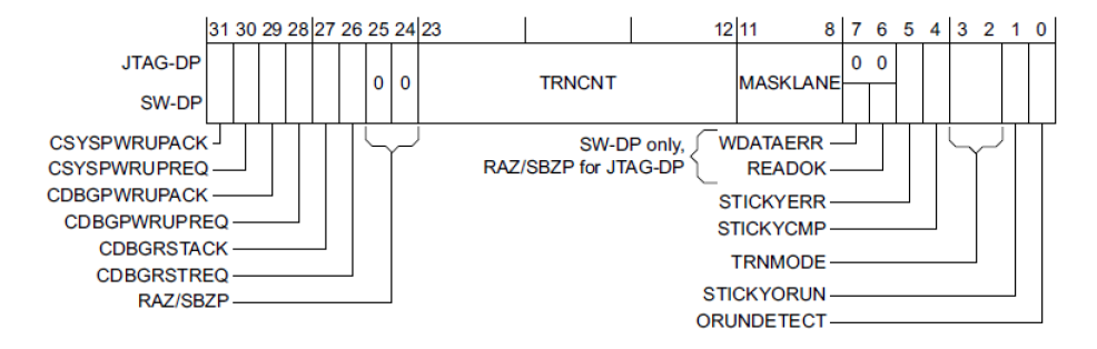
The CTRL/STAT register provides control of the DP and several status bits.
The debugger must write a 1 to the CDBGPWRUPREQ and CSYSPWRUPREQ bits before using the AHB-AP.
The STICKYERR bit is set if an error occurs in a AP transaction.
While the STICKYERR bit is set any SWD request will return a FAULT response.
To clear the STICKYERR bit, use the ABORT register.
Figure 2.4. Control/Status Register (from [adi5])
The SELECT register is used to select which Access Port (AP) is used
when performing an AP transaction (AP bit of request is 1).
The DP can be connected to several APs and this register is u sed to select which one is accessed.
The APSEL field (bits [31:24]) is used to choose between different APs (refer to Figure 1.1 (p. 2) ).
On the EFM32, only one AP is used, the AHB-AP which is selected when APSEL is 0.
As with DP accesses, the request can only select 1 of 4 AP registers with the two address bits.
To allow more registers to be implemented in an AP, the APBANKSEL field of the SELECT register
enables the debugger to specify 4 additional address bits, allowing up to 64 registers to be defined by each AP.
The RDBUFF register returns the result of the previous AP transaction
without generating a new memory access. See Section 2.3 (p. 6) .
2.3 AHB-AP
Table 2.2. AHB-AP registers

The AHB-AP is the only AP present on the EFM32.
It is an implementation of the general MEM-AP, that gives access to the internal memory map of the core.
Since memory, peripherals and debug components are all memory mapped,
the AHB-AP can be used to both program and debug the MCU.
The AHB-AP is selected by writing 0 to the APSEL field of the SELECT register.
This has to be performed before using the AHB-AP as the reset state of the SELECT register is undefined.
Before using the AHBAP the connection should also be verified by reading the IDR register.
The IDR register is at address 0xFC. Thus, to read this register, the APBANKSEL field should be set to 0xF.
The IDR register can then be read by reading register 3 in that register bank (ADDR[3:2] == 0b11). : 0xFC = 1111-1100
The IDR register should return the value 0x24770011 on devices with a Cortex-M3 or Cortex-M4 core.
On devices with a Cortex-M0+ it should return 0x04770031.
If it instead returns the value 0x16E60001, debug access is locked and the AHB-AP is not available.
See Section 4.3 (p. 13) for information on how to unlock a device.
When reading from any AP register, the value in the data phase is from the previous transaction.
That means that in order to read out the value of a register,
it is necessary to perform two reads and discard the first result.
If performing several sequential reads, it is enough to discard the first value and perform one extra read.
The DP register RDBUFF can also be used.
This register will return the result of the last AP read operation without generating a new memory access.
The basic operation on the AHB-AP is to read or write from some memory location.
The two main registers used for this purpose is the Transfer Address Register (TAR)
and the Data Read/Write Register (DRW).
The TAR register contains the address of the resource.
The addressing scheme is the same as the internal memory map of the core.
The DRW register is used to either write or read from the address held in TAR.
To write a value to an internal memory address, first write the address to the TAR register, then write the value to DRW.
To read a memory address, first write the address to TAR, then read the value in DRW.
Figure 2.5. Control/Status Word Register
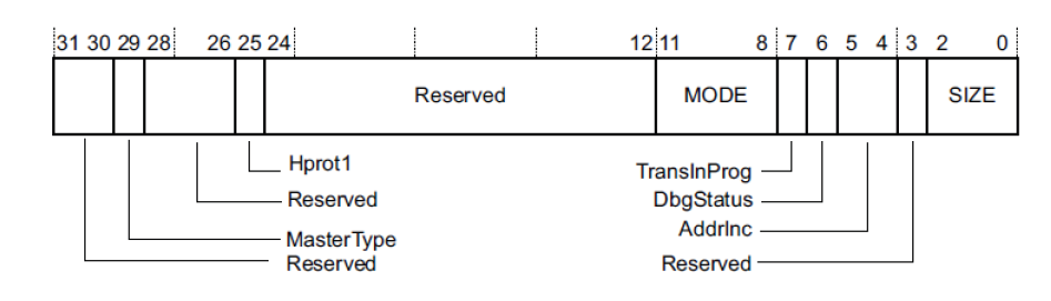
The Control/Status Word (CSW) register contains configuration and status signals about the connection to the internal memory bus.
Before using AHB-AP to read/write to the internal memory, the SIZE field should be set to configure the size of the memory transfer.
The TransInProg bit can be checked to see if a memory transaction is currently in progress.
In summary, when using the AHB-AP:
- 1. Set the CDBGPWRUPREQ and CSYSPWRUPREQ bits of
SW-DP registers CTRL/STATUS (power up the debug interface) - 2. Write 0x000000F0 to SELECT (select AHB-AP, bank 0xF)
- 3. Read the IDR register
- 4. Verify that the IDR value is one of the valid values
- 5. Write 0x00000000 to SELECT (select AHB-AP, bank 0x0)
- 6. Set the SIZE field of CSW to 0x2 (32-bit transfers)
- 7. Start using TAR/DRW to access internal memory
2.4 SEGGER J-Link
All Energy Micro Development and Starter Kits come with an integrated SEGGER J-Link debugger.
The J-Link debugger handles the SWD connection to the EFM32 and communicates with a PC over a USB cable.
The interface on the PC is in the form of a shared library, the JLinkARM.dll.
Applications such as the energyAware Commander and IDEs can use this library to connect to the EFM32 directly.
To use JLinkARM.dll in an application, an SDK (Software Development Kit) must be obtained from Segger.
Figure 2.6. Read IDCODE and IDR with JLink.exe
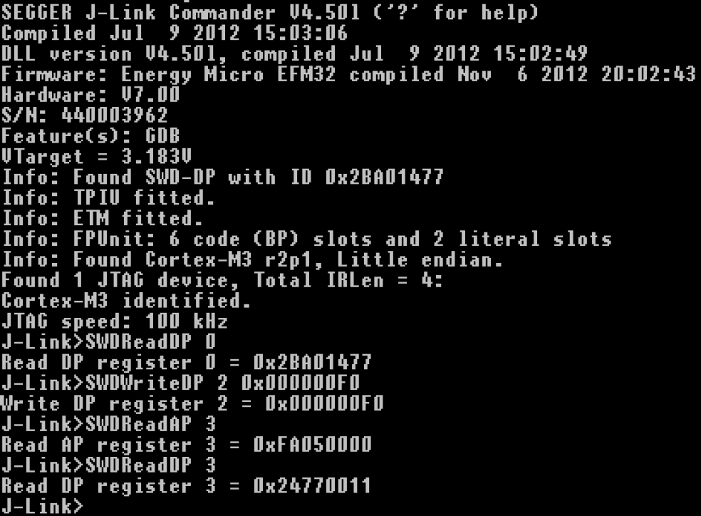
The SEGGER distribution also contains a Command Line Interface (CLI) to directly send SWD commands to the EFM32.
The program is called JLink Commander (JLink.exe).
Figure 2.6 (p. 7) shows a sample JLink Commander session in where the IDCODE and IDR registers are read.
Note that when reading the AP IDR register, a dummy read is performed first,
followed by reading the actual value from the DP RDBUFF register.
The Energy Micro kits can also be used to debug external boards.
If 'Debug Mode' in energyAware Commander is set to 'Out',
the SWD lines are disconnected from the on-board MCU and instead put out on the Debug Header.
The Debug Header can be directly connected to the target board with a standard 20-pin flat cable,
or if the external board does not contain a 20-pin debug header,
it is enough to connect SWDIO, SWCLK, RESET, GND and Vtarget.
3 Flash Programming
To load a program on the EFM32 it must be written to flash.
This chapter will explain how to use the MSC registers to write data to the internal flash of an EFM32.
3.1 Halting the CPU
Before writing a new program to Flash, the CPU should first be reset and halted.
There are two reasons for doing this:
- 1. Get the CPU and peripherals into a known state
- 2. Prohibit the CPU from accidentally running partial code while writing the program
Three registers are used to get to this state.
All of these registers are described in [cm3trm]
- The Debug Halting Control and Status Register (DHCSR).
- The Application Interrupt and Reset Control Register (AIRCR).
- The Debug Exception and Monitor Control Register (DEMCR).
The process is as follows:
- 1. Write 0xA05F0003 to DHCSR. This will halt the core.
- 2. Write 1 to bit VC_CORERESET in DEMCR. This will enable halt-on-reset
- 3. Write 0xFA050004 to AIRCR. This will reset the core and halt.
Now the CPU will be halted on the first instruction and all peripherals
and registers (except for the debug registers) will have their reset value.
3.2 Writing to Flash
Writes to flash (and erase operations) are controlled by the MSC (Memory System Controller) registers.
These registers are described in the EFM32 Reference Manual. The minimum write unit is one word (32 bits).
The following process outlines how to write a word to flash:
- 1. Enable flash writing by setting the WREN bit in MSC_WRITECTRL
- 2. Write the destination address to MSC_ADDRB
- 3. Load the internal write register by writing a 1 to bit LADDRIM in MSC_WRITECMD
- 4. Write the word to MSC_WDATA
- 5. Initiate the write by writing a 1 to bit WRITEONCE in MSC_WRITECMD
This will initiate the write process.
The process takes about 20 μs and the status can be checked by polling the BUSY flag in MSC_STATUS.
The Memory System Controller also supports automatic address increments when writing multiple words.
Use the WRITETRIG bit instead of WRITEONCE to start the write process in order to trigger address increments.
The WDATAREADY flag in MSC_STATUS is used to signal when MSC_WDATA is ready for the next word.
Note that address increments only works within a flash page.
When writing to the last word of a page, the address will wrap around to the start of the current page.
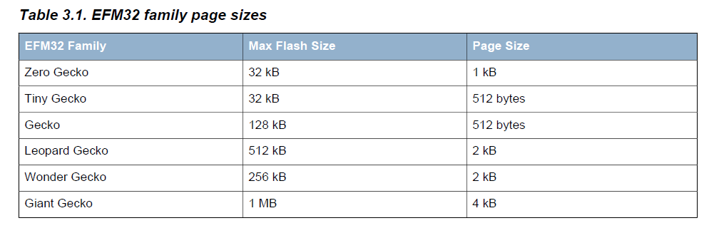
Different EFM32 families have different page sizes. Page sizes are documented in the Reference Manual for each device family.
It is also possible to read out the size of memory and page size directly from the Device Information (DI) page on the MCU.
Table 3.1 (p. 10) shows page sizes for the current EFM32 families at the time of writing.
The process to erase a page is very similar to writing a word.
The start address of the page should be written to MSC_ADDRB
and the bit ERASEPAGE is used instead of WRITEONCE/WRITETRIG to start the erase operation.
The process can be monitored with the BUSY bit in MSC_STATUS.
When a page is erased all bits are 1, i.e. all words are 0xFFFFFFFF.
When writing to flash it is only possible to clear bits (set them to 0).
It is possible to write twice to the same word as long as the bits are either untouched or changed from 1 to 0.
Note that you should not write more than two times to the same word between each erase, even if you follow this rule.
3.3 Using a Flashloader
There are two main strategies that can be used when programming flash.
The first option is to write directly to the MSC registers over the SWD interface.
This is the simplest approach, but also the slowest.
A faster method is to first write a small program directly to RAM and then let this program control the MSC registers.
Such a program is called a flashloader.
This approach is faster because the debugger does not have to continiously check the MSC_STATUS register
before writing a new word.
A large buffer can be written directly to RAM and the flashloader can take care of polling and feeding the MSC,
in addition to signaling the debugger when the buffer can be refilled.
When using a flashloader, the debugger must communicate with the flashloader to know when it is safe to send more data.
The communication can be implemented by using fixed-address variables that both parties check.
The flashloader can be written directly to RAM.
The source code examples provided with this application note (see Chapter 5 (p. 16) )
implements both strategies for programming the target.
To see the speed benefits of using a flashloader, consider the following benchmark:
on an EFM32GG990F1024, a 512 kB firmware image was programmed and verified by both methods.
Without flashloader: 12 kB/s.
With flashloader: 85 kB/s.
3.4 Lock Bits
The Lock Bits (LB) page can be used to lock specific pages of the flash to prevent them from beeing overwritten.
Each flash page has a corresponding bit in the LB page.
If the Lock Bit for a particular page is cleared (set to zero), any write or erase command to that page will be ignored.
The lock bits are grouped in words, so the first word of the LB page contains lock bits for the first 32 pages of the main flash.
The LB page has its own Lock Bit as well, which is also part of the LB page itself.
When this bit is cleared the LB page cannot be erased or written to, which will fix the set of locked flash pages.
However, note that when in Debug Mode (when DBGPWRUPACK in CTRL/STAT is set),
the LB page is writeable regardless of the LB page Lock Bit.
This means that a debugger can connect and change the state of the lock page, even though the LB Page Lock Bit is cleared.
The Lock Bits are documented in the EFM32 Reference Manual.
5 Source Code Example
This application note comes with a source code example which implements a simple programmer by bit-banging GPIO pins.
Projects are included for the EFM32GG-STK3700 and EFM32GG-DK3750.
The following features are demonstrated:
• Program by writing directly to MSC
• Program by using a flashloader
• Lock target
• Unlock target
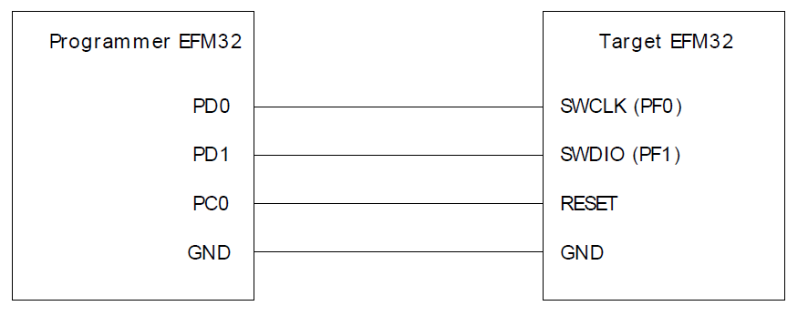
To use the programmer connect RESET, SWCLK, SWDIO and GND from the target to the configured pins on the programmer.
Figure 5.1 (p. 16) shows the default configuration when using the EFM32GG-STK3700.
The voltage level (e.g. 3.3V) should be the same on both host and target.
The pins can be configured in dap.h
Figure 5.1. Default Programmer Connection EFM32GG-STK3700
The program is operated by using PB0 to select an action and PB1 to execute the current action.
The segmented LCD will display information about the current action. LED1 is on when a target is connected.
LED0 is on whenever the programmer is busy with an operation, e.g. programming the target.
More information is output over SWO, which can be viewed by connecting to the kit
with the energyAware Commander and selecting the SWO tab.
/*******************************************************************************
 * @file dap.h
 * @brief Low level SWD interface functions.
 * @author Energy Micro AS
 * @version 1.02
 *******************************************************************************
 * @section License
 * <b>(C) Copyright 2013 Energy Micro AS, http://www.energymicro.com</b>
 *******************************************************************************
 *
 * Permission is granted to anyone to use this software for any purpose,
 * including commercial applications, and to alter it and redistribute it
 * freely, subject to the following restrictions:
 *
 * 1. The origin of this software must not be misrepresented; you must not
 *    claim that you wrote the original software.
 * 2. Altered source versions must be plainly marked as such, and must not be
 *    misrepresented as being the original software.
 * 3. This notice may not be removed or altered from any source distribution.
 * 4. The source and compiled code may only be used on Energy Micro "EFM32"
 *    microcontrollers and "EFR4" radios.
 *
 * DISCLAIMER OF WARRANTY/LIMITATION OF REMEDIES: Energy Micro AS has no
 * obligation to support this Software. Energy Micro AS is providing the
 * Software "AS IS", with no express or implied warranties of any kind,
 * including, but not limited to, any implied warranties of merchantability
 * or fitness for any particular purpose or warranties against infringement
 * of any proprietary rights of a third party.
 *
 * Energy Micro AS will not be liable for any consequential, incidental, or
 * special damages, or any other relief, or for any claim by any third party,
 * arising from your use of this Software.
 *
 *****************************************************************************/
#ifndef _DAP_H_
#define _DAP_H_

/* ACK responses */
#define ACK_OK     1  // 001 : 1 0 0
#define ACK_WAIT   2  // 010 : 0 1 0
#define ACK_FAULT  4  // 100 : 0 0 1

/* Address of DP read registers */
#define DP_IDCODE  0
#define DP_CTRL    1
#define DP_RESEND  2
#define DP_RDBUFF  3

/* Adressses of DP write registers */
#define DP_ABORT   0
#define DP_STAT    1
#define DP_SELECT  2

/* AHB-AP registers */
#define AP_CSW 0
#define AP_TAR 1
#define AP_DRW 3
#define AP_IDR 3  /* In bank 0xf : 0xF3 */

/* AAP registers */
#define AAP_CMD    0
#define AAP_CMDKEY 1
#define AAP_STATUS 2
#define AAP_IDR    3  /* In bank 0xf : 0xF3 */

#define AAP_CMD_ZERO      0xF0E00000
#define AAP_CMDKEY_ZERO   0xF0E00004
#define AAP_STATUS_ZERO   0xF0E00008
#define AAP_IDR_ZERO      0xF0E000FC

/* Valid values for the DP IDCODE register */
#define EFM32_DPID_1      0x2BA01477  // G, LG, GG, TG, WG
#define EFM32_DPID_2      0x0BC11477  // ZG
#define EFM32_DPID_3      0x0bc12477  // SWMD

/* Valid value for the AAP IDR register */
#define EFM32_AAP_ID    0x16e60001

/* Valid values for the AHB-AP IDR register */
#define EFM32_AHBAP_ID_1  0x24770011 // G, LG, GG, TG, WG
#define EFM32_AHBAP_ID_2  0x04770031 // ZG

/* Key which must be written to AAP_CMDKEY before
 * writing to AAP_CMD */
#define AAP_UNLOCK_KEY 0xcfacc118

/* Value to write to AIRCR in order to do a soft
 * reset of the target */
#define AIRCR_RESET_CMD 0x05FA0006

/* Bit fields for the CSW register */
#define AP_CSW_32BIT_TRANSFER   0x02
#define AP_CSW_AUTO_INCREMENT   0x10
#define AP_CSW_MASTERTYPE_DEBUG (1 << 29)
#define AP_CSW_HPROT            (1 << 25)
#define AP_CSW_DEFAULT (AP_CSW_32BIT_TRANSFER | AP_CSW_MASTERTYPE_DEBUG | AP_CSW_HPROT)

/* Powerup request and acknowledge bits in CTRL/STAT */
#define DP_CTRL_CDBGPWRUPREQ  (1 << 28)
#define DP_CTRL_CDBGPWRUPACK  (1 << 29)
#define DP_CTRL_CSYSPWRUPREQ  (1 << 30)
#define DP_CTRL_CSYSPWRUPACK  (1 << 31)

/* Commands to run/step and let CPU run.
 * Write these to DHCSR */
#define RUN_CMD  0xA05F0001
#define STOP_CMD 0xA05F0003
#define STEP_CMD 0xA05F0005

/* Flash addresses to retrieve the device unique id */
#define UNIQUE_ID_HIGH_ADDR 0x0FE081F4
#define UNIQUE_ID_LOW_ADDR  0x0FE081F0

/* AAP bit fields */
#define AAP_CMD_DEVICEERASE 1
#define AAP_CMD_SYSRESETREQ 2
#define AAP_STATUS_ERASEBUSY 1

/* Default pin configuration is provided
 * for EFM32GG-STK3700 and EFM32GG-DK3750.
 * Change these defines to select other pins.
 * Note that in order to perform the
 * Gecko Unlock Sequence, the pins PE8,PE9
 * MUST be used for SWCLK,SWDIO.
 */
#if defined(STK)

#define SWCLK_PORT 3
#define SWCLK_PIN  0
#define SWDIO_PORT 3
#define SWDIO_PIN  1
#define RESET_PORT 2
#define RESET_PIN  0

#else

#define SWCLK_PORT 4
#define SWCLK_PIN  8
#define SWDIO_PORT 4
#define SWDIO_PIN  9
#define RESET_PORT 2
#define RESET_PIN  0

#endif

/* Number of times to retry an SWD operation when receiving a WAIT response */
#define SWD_RETRY_COUNT 200

/* Number of times to retry the connection sequence */
#define CONNECT_RETRY_COUNT 3

/* Number of times to retry reading the AHB-IDR register when connecting */
#define AHB_IDR_RETRY_COUNT 20

/* Number of times to retry the AAP window expansion sequence (with longer and longer delays) */
#define AAP_EXPANSION_RETRY_COUNT 50

/* Number of times to retry reading the CTLR/STAT register while waiting for powerup acknowledge */
#define PWRUP_TIMEOUT 100

/* Number of times to retry reading the ERASEBUSY flag while waiting for Mass Erase (Debug Unlock) to complete */
#define UNLOCK_RETRY_COUNT 5

/* Number of times to retry reading status registers while waiting for a debug event (such as a halt of soft reset) */
#define DEBUG_EVENT_TIMEOUT 200

/* Number of times to wait for flashloader */
#define FLASHLOADER_RETRY_COUNT 1000

/* Number of times to wait for MSC operation to complete */
#define MSC_TIMEOUT 100

/* JTAG to SWD bit sequence, transmitted LSB first */
#define JTAG2SWD 0xE79E

#if (SWDIO_PIN < 8)
#define SWDIO_SET_INPUT() { \
    GPIO->P[SWDIO_PORT].MODEL = (GPIO->P[SWDIO_PORT].MODEL & ~(0xf << 4 * SWDIO_PIN)) | (0x1 << (4 * SWDIO_PIN)); \
    GPIO->P[SWDIO_PORT].DOUT &=  ~(1 << SWDIO_PIN); }
#else
#define SWDIO_SET_INPUT() { \
    GPIO->P[SWDIO_PORT].MODEH = (GPIO->P[SWDIO_PORT].MODEH & ~(0xf << 4 * (SWDIO_PIN-8))) | (0x1 << (4 * (SWDIO_PIN-8))); \
    GPIO->P[SWDIO_PORT].DOUT &=  ~(1 << SWDIO_PIN); }
#endif

#if (SWDIO_PIN < 8)
#define SWDIO_SET_OUTPUT() { \
    GPIO->P[SWDIO_PORT].MODEL = (GPIO->P[SWDIO_PORT].MODEL & ~(0xf << 4 * SWDIO_PIN)) | (0x4 << (4 * SWDIO_PIN)); \
    GPIO->P[SWDIO_PORT].DOUT &=  ~(1 << SWDIO_PIN); }
#else
#define SWDIO_SET_OUTPUT() { \
    GPIO->P[SWDIO_PORT].MODEH = (GPIO->P[SWDIO_PORT].MODEH & ~(0xf << 4 * (SWDIO_PIN-8))) | (0x4 << (4 * (SWDIO_PIN-8))); \
    GPIO->P[SWDIO_PORT].DOUT &=  ~(1 << SWDIO_PIN); }
#endif

#define SWDIO_SET() GPIO->P[SWDIO_PORT].DOUT |= (1 << SWDIO_PIN)
#define SWDIO_CLR() GPIO->P[SWDIO_PORT].DOUT &= ~(1 << SWDIO_PIN)
#define SWCLK_SET() GPIO->P[SWCLK_PORT].DOUT |= (1 << SWCLK_PIN)
#define SWCLK_CLR() GPIO->P[SWCLK_PORT].DOUT &= ~(1 << SWCLK_PIN)

#define SWDIO_OUT(bit) {if ( bit ) SWDIO_SET(); else SWDIO_CLR();}
#define SWDIO_IN() ((GPIO->P[SWDIO_PORT].DIN >> SWDIO_PIN) & 0x1)

// IDLE : SWDIO ouptput 0, SWCLK output 1

// SWCLK = 0, SWCLK = 1
#define SWCLK_CYCLE()   \
  SWCLK_CLR();          \
  SWCLK_SET()

// SWDIO = 1, SWDIO = 0
#define SWDIO_CYCLE()   \
  SWDIO_SET();          \
  SWDIO_CLR()

/* If SWD_FAST is defined we compile faster versions
 * of the write and read bit macros.
 * Note that the fast macros require that
 * SWCLK and SWDIO is on the same GPIO port
 * and also that the RESET line is NOT connected
 * to this port since the macros write to the
 * entire port at once.
 */
#ifdef SWD_FAST

// Write SWDIO, SWCLK = 0, SWCLK = 1 : Target Capture SWDIO
#define WRITE_BIT(bit) \
if ( bit ) { \
  GPIO->P[SWDIO_PORT].DOUT = (1 << SWDIO_PIN); \
  GPIO->P[SWDIO_PORT].DOUT = (1 << SWDIO_PIN) | (1 << SWCLK_PIN); \
} else { \
  GPIO->P[SWDIO_PORT].DOUT = 0;  \
  GPIO->P[SWDIO_PORT].DOUT = 1 << SWCLK_PIN; \
}

// SWCLK = 0, Read Clocked SWDIO, SWCLK = 1, Target Clock Next Bit
#define READ_BIT(bit)                           \
  GPIO->P[SWCLK_PORT].DOUT = 0;                 \
  bit = SWDIO_IN();                             \
  GPIO->P[SWCLK_PORT].DOUT = 1 << SWCLK_PIN

#else

#define WRITE_BIT(bit)  \
  SWDIO_OUT(bit)        \
  SWCLK_CLR();          \
  SWCLK_SET();

#define READ_BIT(bit)   \
  SWCLK_CLR();          \
  bit = SWDIO_IN();     \
  SWCLK_SET()

#endif

void JTAG_to_SWD_Sequence( void );
void writeAP( int reg, uint32_t data );
void writeDP( int reg, uint32_t data );
void readAP( int reg, uint32_t *data );
void readDP( int reg, uint32_t *data );
uint32_t initDp( void );
uint32_t readApId( void );
void aapExtensionSequence( void );

#endif
/*******************************************************************************
 * @file dap.c
 * @brief Low level SWD interface functions.
 * @author Energy Micro AS
 * @version 1.02
 *******************************************************************************
 * @section License
 * <b>(C) Copyright 2013 Energy Micro AS, http://www.energymicro.com</b>
 *******************************************************************************
 *
 * Permission is granted to anyone to use this software for any purpose,
 * including commercial applications, and to alter it and redistribute it
 * freely, subject to the following restrictions:
 *
 * 1. The origin of this software must not be misrepresented; you must not
 *    claim that you wrote the original software.
 * 2. Altered source versions must be plainly marked as such, and must not be
 *    misrepresented as being the original software.
 * 3. This notice may not be removed or altered from any source distribution.
 * 4. The source and compiled code may only be used on Energy Micro "EFM32"
 *    microcontrollers and "EFR4" radios.
 *
 * DISCLAIMER OF WARRANTY/LIMITATION OF REMEDIES: Energy Micro AS has no
 * obligation to support this Software. Energy Micro AS is providing the
 * Software "AS IS", with no express or implied warranties of any kind,
 * including, but not limited to, any implied warranties of merchantability
 * or fitness for any particular purpose or warranties against infringement
 * of any proprietary rights of a third party.
 *
 * Energy Micro AS will not be liable for any consequential, incidental, or
 * special damages, or any other relief, or for any claim by any third party,
 * arising from your use of this Software.
 *
 *****************************************************************************/
#include <stdint.h>
#include <stdbool.h>
#include <stdio.h>
#include <setjmp.h>
#include "em_device.h"
#include "em_cmu.h"
#include "em_gpio.h"
#include "dap.h"
#include "errors.h"

/* These codes are only needed for SWD protocol version 2 with multidrop */
static uint32_t selectionAlertSequence[ ] =
{ 0x6209F392, 0x86852D95, 0xE3DDAFE9, 0x19BC0EA2 };
static uint32_t activationCode = 0x1A;

/**********************************************************
 * Reads from an AP or DP register.
 *
 * @param ap
 *   If this parameter is true, read from AP register.
 *   If false read from DP register.
 *
 * @param reg
 *   The register number [0-3] to read from
 *
 * @param data[out]
 *   The register value is written to this parameter
 **********************************************************/
static uint32_t readReg( bool ap, int reg, uint32_t *data )
{
  int i;
  uint32_t cb = 0;
  uint32_t parity;
  uint32_t b;
  uint32_t ack = 0;
  uint32_t ret = SWD_ERROR_OK;

  /* Initalize output variable */
  *data = 0;

  /* Convert to int */
  int _ap = (int) ap;
  int _read = (int) 1;

  int A2 = reg & 0x1;
  int A3 = ( reg >> 1 ) & 0x1;

  /* Calulate parity */
  parity = ( _ap + _read + A2 + A3 ) & 0x1;

  SWDIO_SET_OUTPUT( );

  /* Send request */
  WRITE_BIT( 1 );
  WRITE_BIT( _ap );
  WRITE_BIT( _read );
  WRITE_BIT( A2 );
  WRITE_BIT( A3 );
  WRITE_BIT( parity );
  WRITE_BIT( 0 );
  WRITE_BIT( 1 );   // SWDIO = 1, SWCLK = 0, SWCLK = 1

  /* Turnaround */
  SWDIO_SET_INPUT( );
  SWCLK_CYCLE( );  // SWCLK = 0, SWCLK = 1 : Target Output First Bit : Rising Edge

  /* Read ACK */
  for ( i = 0; i < 3; i++ )
  {
    READ_BIT( b );  // SWCLK = 0, b = SWDIO, SWCLK = 1 : Output Next Bit : Rising Edge
    ack |= b << i;
  }

  /* Verify that ACK is OK */
  if ( ack == ACK_OK )  // First Data Bit Output to Read
  {
    for ( i = 0; i < 32; i++ )
    {
      /* Read bit */
      READ_BIT( b );    // SWCLK = 0, b = SWDIO, SWCLK = 1 : Output Next Bit : Rising Edge
      *data |= b << i;

      /* Keep track of expected parity */
      if ( b )
        cb = !cb;
    }

    /* Read parity bit */
    READ_BIT( parity ); // Parity Bit Clocked out before SWCLK = 1, this Rising Edge Target will Relase SWDIO

    /* Verify parity */
    if ( cb == parity )
    {
      ret = SWD_ERROR_OK;
    }
    else
    {
      ret = SWD_ERROR_PARITY;
    }

  }
  else if ( ack == ACK_WAIT )
  {
    ret = SWD_ERROR_WAIT;
  }
  else if ( ack == ACK_FAULT )
  {
    ret = SWD_ERROR_FAULT;
  }
  else
  {
    /* Line not driven. Protocol error */
    ret = SWD_ERROR_PROTOCOL;
  }

  /* Turnaround */
  SWCLK_CYCLE( );  // SWDIO is input, SWCLK = 0, SWCLK = 1

  /* 8-cycle idle period. Make sure transaction is clocked through DAP. */
  SWDIO_SET_OUTPUT( ); // SWDIO is output
  for ( i = 0; i < 8; i++ )
  {
    WRITE_BIT( 0 );
  }

  return ret;   // SWDIO = 0, SWCLK = 1 : IDLE State
}

/**********************************************************
 * Writes to a DP or AP register.
 *
 * @param ap
 *   If this parameter is true, write to AP register.
 *   If false write to DP register.
 *
 * @param reg
 *   The register number [0-3] to write to
 *
 * @param data
 *   The value to write to the register
 **********************************************************/
static uint32_t writeReg( bool ap, int reg, uint32_t data, bool ignoreAck )
{
  uint32_t ack = 0;
  int i;
  uint32_t parity = 0;
  uint32_t b;
  uint32_t ret = SWD_ERROR_OK;

  /* Convert to int */
  int _ap = (int) ap;
  int _read = (int) 0;

  /* Calulate address bits */
  int A2 = reg & 0x1;
  int A3 = ( reg >> 1 ) & 0x1;

  /* Calculate parity */
  parity = ( _ap + _read + A2 + A3 ) & 0x1;

  SWDIO_SET_OUTPUT( );

  /* Write request */
  WRITE_BIT( 1 );
  WRITE_BIT( _ap );
  WRITE_BIT( _read );
  WRITE_BIT( A2 );
  WRITE_BIT( A3 );
  WRITE_BIT( parity );
  WRITE_BIT( 0 );
  WRITE_BIT( 1 );

  SWDIO_SET_INPUT( );

  /* Turnaround */
  SWCLK_CYCLE( );

  /* Read acknowledge */
  for ( i = 0; i < 3; i++ )
  {
    READ_BIT( b );
    ack |= b << i;
  }

  if ( ack == ACK_OK || ignoreAck )
  {
    /* Turnaround */
    SWCLK_CYCLE( );

    SWDIO_SET_OUTPUT( );

    /* Write data */
    parity = 0;
    for ( i = 0; i < 32; i++ )
    {
      b = ( data >> i ) & 0x1;
      WRITE_BIT( b );
      if ( b )
        parity = !parity;
    }

    /* Write parity bit */
    WRITE_BIT( parity );

  }
  else if ( ack == ACK_WAIT )
  {
    ret = SWD_ERROR_WAIT;
  }
  else if ( ack == ACK_FAULT )
  {
    ret = SWD_ERROR_FAULT;
  }
  else
  {
    /* Line not driven. Protocol error */
    ret = SWD_ERROR_PROTOCOL;
  }

  /* 8-cycle idle period. Make sure transaction
   * is clocked through DAP. */
  SWDIO_SET_OUTPUT( );
  for ( i = 0; i < 8; i++ )
  {
    WRITE_BIT( 0 );
  }

  return ret;

}

/**********************************************************
 * Sends the JTAG-to-SWD sequence. This must be performed
 * at the very beginning of every debug session and
 * again in case of a protocol error.
 **********************************************************/
void JTAG_to_SWD_Sequence( void )
{
  int i;
  int b;

  SWDIO_SET_OUTPUT( );

  /* First reset line with > 50 cycles with SWDIO high */
  SWDIO_OUT( 1 );
  for ( i = 0; i < 60; i++ )
  {
    SWCLK_CYCLE( );
  }

  /* Transmit 16-bit JTAG-to-SWD sequence */
  for ( i = 0; i < 16; i++ )
  {
    b = ( JTAG2SWD >> i ) & 0x1;
    WRITE_BIT( b );
  }

  /* Do another reset to make sure SW-DP is in reset state */
  SWDIO_OUT( 1 );
  for ( i = 0; i < 60; i++ )
  {
    SWCLK_CYCLE( );
  }

  /* Insert a 16 cycle idle period */
  SWDIO_OUT( 0 );
  for ( i = 0; i < 16; i++ )
  {
    SWCLK_CYCLE( );
  }
}

/**********************************************************
 * This function is used to take the target DAP from
 * 'dormant' state to 'reset' state. It is only used
 * on DAPs that implement SWD protocol version 2 (or
 * later) that implements multidrop.
 **********************************************************/
void exitDormantState( void )
{
  int i, j, b;

  SWDIO_SET_OUTPUT( );

  /* At least 8 cycles with SWDIO high */
  for ( i = 0; i < 10; i++ )
  {
    WRITE_BIT( 1 );
  }

  /* 128-bt selection alert sequence */
  for ( i = 0; i < 4; i++ )
  {
    for ( j = 0; j < 32; j++ )
    {
      b = ( selectionAlertSequence[ i ] >> j ) & 0x1;
      WRITE_BIT( b );
    }
  }

  /* Four cycles with SWDIO low */
  for ( i = 0; i < 4; i++ )
  {
    WRITE_BIT( 0 );
  }

  /* Serial Wire Activation code */
  for ( i = 0; i < 8; i++ )
  {
    b = ( activationCode >> i ) & 0x1;
    WRITE_BIT( b );
  }

  /* Line reset */
  for ( i = 0; i < 60; i++ )
  {
    WRITE_BIT( 1 );
  }
}

/**********************************************************
 * Writes to one of the four AP registers in the currently
 * selected AP bank.
 *
 * @param reg[in]
 *    The register number [0-3] to write to
 *
 * @param data[in]
 *    Value to write to the register
 *
 **********************************************************/
void writeAP( int reg, uint32_t data )
{
  uint32_t swdStatus;
  uint32_t retry = SWD_RETRY_COUNT;

  do
  {
    swdStatus = writeReg( true, reg, data, false );
    retry--;
  }while ( swdStatus == SWD_ERROR_WAIT && retry > 0 );

  if ( swdStatus != SWD_ERROR_OK )
  {
    RAISE( swdStatus );
  }
}

/**********************************************************
 * Writes to one of the four DP registers.
 *
 * @param reg[in]
 *    The register number [0-3] to write to
 *
 * @param data[in]
 *    Value to write to the register
 *
 **********************************************************/
void writeDP( int reg, uint32_t data )
{
  uint32_t swdStatus;
  uint32_t retry = SWD_RETRY_COUNT;

  do
  {
    swdStatus = writeReg( false, reg, data, false );
    retry--;
  }while ( swdStatus == SWD_ERROR_WAIT && retry > 0 );

  if ( swdStatus != SWD_ERROR_OK )
  {
    RAISE( swdStatus );
  }
}

/**********************************************************
 * Writes to one of the four DP registers and ignores
 * the ACK response. This is needed when writing
 * to the TARGETSEL register.
 *
 * @param reg[in]
 *    The register number [0-3] to write to
 *
 * @param data[in]
 *    Value to write to the register
 *
 **********************************************************/
void writeDpIgnoreAck( int reg, uint32_t data )
{
  uint32_t swdStatus;
  uint32_t retry = SWD_RETRY_COUNT;

  do
  {
    swdStatus = writeReg( false, reg, data, true );
    retry--;
  }while ( swdStatus == SWD_ERROR_WAIT && retry > 0 );

  if ( swdStatus != SWD_ERROR_OK )
  {
    RAISE( swdStatus );
  }
}

/**********************************************************
 * Reads one of the four AP registers in the currently
 * selected AP bank.
 *
 * @param reg[in]
 *    The register number [0-3] to read
 *
 * @param data[out]
 *    Value of register is written to this parameter
 *
 **********************************************************/
void readAP( int reg, uint32_t *data )
{
  uint32_t swdStatus;
  uint32_t retry = SWD_RETRY_COUNT;

  do
  {
    swdStatus = readReg( true, reg, data );
    retry--;
  }while ( swdStatus == SWD_ERROR_WAIT && retry > 0 );

  if ( swdStatus != SWD_ERROR_OK )
  {
    RAISE( swdStatus );
  }
}

/**********************************************************
 * Reads one of the four DP registers.
 *
 * @param reg[in]
 *    The register number [0-3] to read
 *
 * @param data[out]
 *    Value of register is written to this parameter
 *
 **********************************************************/
void readDP( int reg, uint32_t *data )
{
  uint32_t swdStatus;
  uint32_t retry = SWD_RETRY_COUNT;

  do
  {
    swdStatus = readReg( false, reg, data );
    retry--;
  }while ( swdStatus == SWD_ERROR_WAIT && retry > 0 );

  if ( swdStatus != SWD_ERROR_OK )
  {
    RAISE( swdStatus );
  }
}

/**********************************************************
 * Initalized the SW-DP. This function performs first
 * sends the JTAG-to-SWD sequence and then reads
 * the IDCODE register.
 *
 * @returns
 *    The value of the IDCODE register
 **********************************************************/
uint32_t initDp( void )
{
  uint32_t dpId;

  /* If connecting to a Multidrop capable SW-DP (SWD version 2), this
   * function must be run first. */
  //exitDormantState();
  /* Send the JTAG-to-SWD switching sequence */
  JTAG_to_SWD_Sequence( );

  /* Read IDCODE to get the DAP out of reset state */
  readDP( DP_IDCODE, &dpId );

  /* Debug power up request */
  writeDP( DP_CTRL, DP_CTRL_CSYSPWRUPREQ | DP_CTRL_CDBGPWRUPREQ );

  /* Wait until we receive powerup ACK */
  int retry = PWRUP_TIMEOUT + 200;
  uint32_t status;
  while ( retry > 0 )
  {
    readDP( DP_CTRL, &status );
    if ( ( status & ( DP_CTRL_CDBGPWRUPACK | DP_CTRL_CSYSPWRUPACK ) )
      == ( DP_CTRL_CDBGPWRUPACK | DP_CTRL_CSYSPWRUPACK ) )
    {
      break;
    }

    retry--;
  }

  /* Throw error if we failed to power up the debug interface */
  if ( ( status & ( DP_CTRL_CDBGPWRUPACK | DP_CTRL_CSYSPWRUPACK ) )
    != ( DP_CTRL_CDBGPWRUPACK | DP_CTRL_CSYSPWRUPACK ) )
  {
    RAISE( SWD_ERROR_DEBUG_POWER );
  }

  /* Select first AP bank */
  writeDP( DP_SELECT, 0x00 );

  return dpId;
}

/**********************************************************
 * Reads the ID of AP #0. This will be either
 *   - EFM32_AHBAP_ID  if device is unlocked
 *   - EFM32_AAP_ID    if device is locked
 *
 * Note: on Zero Gecko it will always be EFM32_AHBAP_ID
 * and the AAP must be access as a memory mapped peripheral
 *
 * @returns
 *    The value of IDR register (address 0xFC) for AP #0
 **********************************************************/
uint32_t readApId( void )
{
  uint32_t apId;

  /* Select last AP bank */
  writeDP( DP_SELECT, 0xf0 );

  /* Dummy read AP ID */
  readAP( AP_IDR, &apId );

  /* Read AP ID */
  readDP( DP_RDBUFF, &apId );

  /* Select first AP bank again */
  writeDP( DP_SELECT, 0x00 );

  return apId;
}

/**********************************************************
 * Sends the AAP Window Expansion Sequence. This sequence
 * should be sent on SWDIO/SWCLK when reset is held low.
 * This will cause the AAP window to be 255 times longer
 * when reset is released.
 **********************************************************/
void aapExtensionSequence( void )
{
  int i;

  SWCLK_SET( );

  for ( i = 0; i < 4; i++ )
  {
    SWDIO_CYCLE( );
  }

  SWCLK_CLR( );

  for ( i = 0; i < 4; i++ )
  {
    SWDIO_CYCLE( );
  }

  SWCLK_CLR( );
}

/**********************************************************
 * Initalize the AHB-AP. The transfer size must be set
 * to 32-bit before trying to access any internal
 * memory.
 **********************************************************/
void initAhbAp( void )
{
  /* Set transfer size to 32 bit */
  writeAP( AP_CSW, AP_CSW_DEFAULT );
}

