
Vehicle Network Protocols -- ISO/KWP CAN CCD PCI SCI / SCP / Class 2
Vehicle Network Protocols
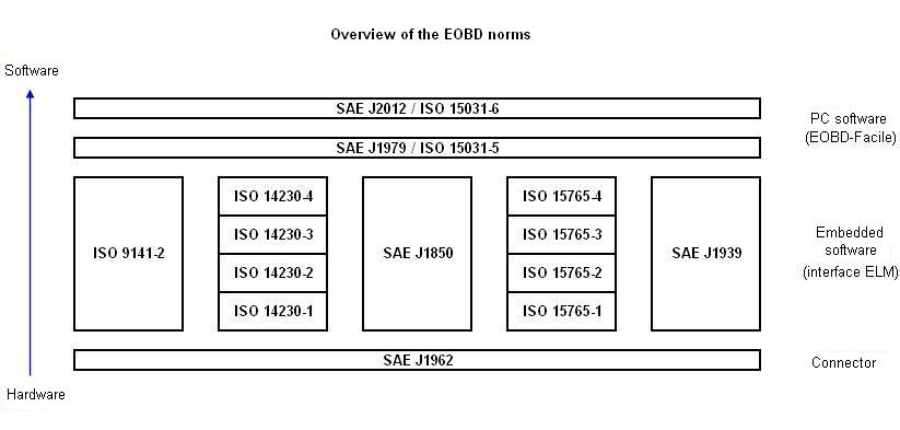
There are 5 protocols in the OBD2 system and a car will normally only use 1 of them
PROTOCOLS
J1850 PWM (pulse width modulation) used by Ford Motor Company and Mazda
J1850 VPW (variable width modulation) used by General Motors and in light trucks
ISO9141-2 = older protocol in Chrysler, European, and Asian vehicles between 2000-2004
ISO14230-4 KWP2000 (keyword protocol 2000) commonly used in cars from 2003
ISO 15765-4 CAN-BUS = first introduced in 2004 then mandatory in all vehicles from 2008
NOTE: There are 4 variations of CAN-BUS detailed below: each with different length and bus speed
(1) ISO 15765-4 CAN (11 bit ID,500 Kbaud)
(2) ISO 15765-4 CAN (29 bit ID,500 Kbaud)
(3) ISO 15765-4 CAN (11 bit ID,250 Kbaud)
(4) ISO 15765-4 CAN (29 bit ID,250 Kbaud)
The 16 pin diagnostic port normally utilizes only the pins required for the protocol in the car so it’s possible to guess the protocol
with reasonable accuracy by looking at the pins used in the diagnostic port
VPW, metal contacts in pins 2, 4, 5, and 16, but not 10
ISO metal contacts in pins 4, 5, 7, and 16. (15 may or may not be present)
PWM, metal contacts in pins 2, 4, 5, 10, and 16
CAN metal pins in 4, 5, 6, 14, and 16
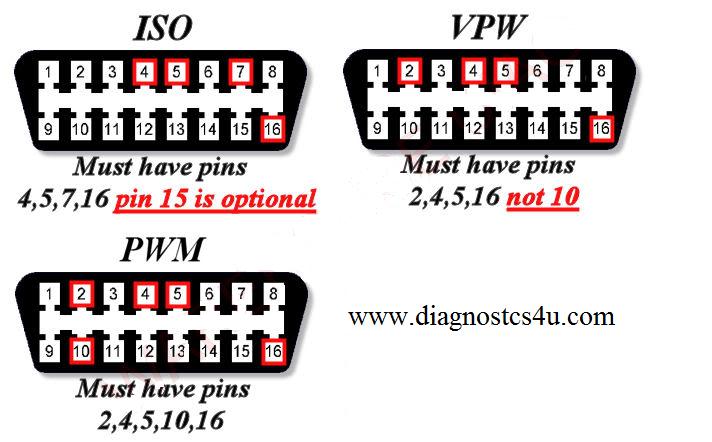
Note:
ISO 9141 and ISO 14230 use the same pinout so you cannot tell the difference between them by just looking at the connector
PIN USE IN NUMBERED ORDER
1 - Discretionary
2 - SAE-J1850 PWM and SAE 1850 VPW positive bus line
3 - Discretionary
4 - Chassis ground (battery negative)
5 - Signal ground (max 1.5 Amp)
6 - ISO-15765-4 CAN (high line) and SAE J2284
7 - K-line of ISO-9141-2 and ISO-14230-4 (data line)
8 - Discretionary
9 - Discretionary
10 - SAE-J1850 (PWM) (negative bus line) (not SAE 1850VPW)
11 – Discretionary
12 - Discretionary
13 - Discretionary
14 - ISO-15765-4 CAN (low line) and SAE J2284)
15 - L-line of ISO-9141-2 and ISO-14230-4
16 - Positive voltage (battery positive, max 4 amps)
Note: None of the 16 pins with the exception of (4) (5) (16) actually have any standard allocation
therefore an ISO9141-2/ISO14230-4 car can use the SAE J1850 pins and vice versa.
The only rule is that when different pin allocations are chosen they must not damage or confuse diagnostic compliant scan/test equipment
Note: Vehicle manufacturers can use the discretionary pins for anything they choose
The list below is but a few of the multiplexing systems in use today. Each system has its differences but for the most part they operate in a similar manner. We will take a brief look at each system including lab-scope waveforms of bus communications.
- Chrysler
- CCD ( Chrysler Collision Detection, 7812.5 Bps )
- PCI ( Programmable Controller Interfacer : SAE J1850 VPW, 10.4 KBps )
- SCI ( Serial Communications Interface : J2610, 62.5 KBps )
- ISO9141 ( 10.4 KBps )
- Ford
- SCP ( Standard Corporate Protocol SAE J1850 PWM, 41.6 KBps )
- ACB/ACP ( Audio Control Bus or Protocol )
- UBP ( UART Based Protocol )
- General Motors
- Class 2 ( SAE J1850 VPW, 10.4 KBps or 41.6 KBps in special diagnostic mode )
- ALDL ( Assembly Line Diagnostic Link, 8192 UART )
- GMLAN ( High Speed and Low Speed)
- GMLAN SWC ( Signal Wire CAN, J2411 25 KBps or 80 KBps in special diagnostic mode )
- ISO9141 ISO9141-2 ISO9141 CARB ( 10.4 KBps )
- ISO14230
- ISO11898 ( High Speed CAN )
- ISO11519 ( Low Speed CAN )
Chrysler CCD
Chrysler Collision Detection
- Also called C2D
- Introduced on the 1988 Dodge Dynasty
- Transmission and body control networks
Handles a max of 13 Modules
- 12+ Scan tools
Chrysler Collision Detection, CCD, was one of the fi rst widely used vehicle-wide multiplexing protocols used in the US. Introduced in 1988 on the Dodge Dynasty and Chrysler New Yorker, CCD was originally used for transmission controller to engine controller communications and data sharing. Soon thereafter, body control functions were added to the CCD bus.
CCD Bias Voltage Key Factors:
- Bias voltage provides power to the bus
- Bias voltage varies slightly between vehicles
- Bias supplied by one or more modules, typically by the module that “wakes-up” first
- Bias voltage must be between 1.5 volts and 3.5 volts, otherwise controllers may not be able to interpret messages
CCD Bus Termination
Besides power, the bus also needs ground. The CCD Bus Termination ground is:
- Provided through one or more 120 ohm termination resistors
- Located in one or more modules
- Bias and termination are not necessarily supplied by the same module
CCD Bias and Termination
Bias can be provided by either the BCM, PCM, ETAX, VIC or VTA. Any module can provide termination and the PCM may provide backup termination. If PCM and TCM are the only modules the TCM provides Bias and the PCM provides termination.
CCD Bus Resistance Values
Typical CCD bus resistance values:
- Single termination resistor 100-140 ohms
- Dual termination resistors 40-80 ohms
The termination resistor resistance should not be either 0 ohms or infinity. Without termination, bus voltage will be 5.0 volts on one wire and 0.0 volts on the other. CCD bus termination resistance can be measured with an ohm meter (battery disconnected) at either CCD pin at the DLC. Because the number of termination resistors can vary, an exact resistance specification is not possible. However, the resistance should not read 0 ohms (shorted) or infinity (open). Without termination, bus voltage will be 5.0 volts on one wire and 0.0 volts on the other, as opposed to the proper 2.51 volts on CCD- and 2.49 volts on CCD+.
Testing Note:
Remember when testing the CCD bus that it uses a floating ground, not vehicle ground. To see an accurate representation of the bus voltage on the lab scope you must connect across CCD+ and CCD-, not CCD+ to ground.
The two wires of the CCD bus are connected in parallel; however, the manner in which the connections are made varies. Either standard splices may be used, or the bus can be connected at a joint connector or splice pack. The joint connector can make bus diagnosis significantly easier by having access to all modules on the bus in one location. Splices, on the other hand ,can be located anywhere on the vehicle.
Chrysler PCI Bus ( SAE J1850 VPW )
Introduced in 1998, replaced CCD as a Body Protocol. A vehicle will have either CCD or PCI, not both and PCI is a Single Wire Network. PCI Bus Speed 10.4 kbps and can support up to 32 modules or nodes. It is used as a global OBD-II scan tool interface.
Below is an example of Chrysler PCI communication as viewed on a lab scope. This waveform was captured at pin #2 of the OBD-II DLC. The PCI bus can communicate key off as long as one or modules are still active. The waveform will have an amplitude of 7.0 volts to 7.5 volts.
PCI Bus Diagnosis
A PCI bus shorted to power or ground will cause a total loss of bus communications
A loss of power or ground to an individual node should not affect bus communication. Only that module should be effected. However, an open ground could cause a back feed of voltage to the rest of the bus, potentially interrupting communication to the whole bus. Resistance values determine the module’s dominance on the bus. The lower the resistance, the higher the priority of the module.
- PCM 1000 ohms
- SKIM, ABS, SIR, EVIC 10,500 ohms
- DLC 11,000 ohms
These are typical values and should not be used for actual diagnosis. Actual specifications can be found in your service information system. Here are some tips to remember when testing these PCI circuits.
- Some applications use conventional splices to connect modules to the bus
- Splices can be located anywhere on the vehicle
- In some applications, the BCM acts as a hub for the bus
- Unplugging BCM connectors can help isolate problem modules
- Some applications use a Diagnostic Junction Port (DJP)
- Acts as a centralized splice for the bus
- Every module connected to the DJP can be diagnosed from this location
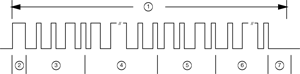
1. Frame
2. Start of Frame
3. Header Message
4. Data Byte(s)
5. CRC Byte
6. In Frame Response bytes
7. End of Frame
Each module can transmit and receive data simultaneously.
A PCI Bus message typically has the following four components:
Message Header - Is one to three bytes in length.
This contains the message type and length, priority, target module(s) and sending module
Data Byte(s) - This is the message that is being sent
Cyclic Redundancy Check (CRC) Byte - This byte is used to detect errors during message transmission
In-Frame Response Byte(s) - If a response is required from the target module(s), it can be sent during this frame
The PCI bus on which we’re focused in this article replaced Chrysler’s earlier two-wire CCD network,
which communicates at slightly less than 8 Kbps.
The PCI is a one-wire network (usually a yellow wire with a purple stripe or vice versa)
that utilizes the slower of the two SAE J1850 protocols (about 10.4 Kbps) switching
between low and high voltage levels to generate signals.
PCI bus low voltage is around zero volts, and high voltage is around 7.5 volts (half of charging system voltage).
The low and high voltage levels on a PCI bus are generated by means of variable-pulse width modulation to form signals of varying length (see illustration).
Each up or down square is a “bit,” and the bus can communicate with up to 10,400 of these pulses every second.
It’s almost insulting to share the obvious fact that you can’t measure these signals with a meter;
use a good fast O-scope set to the 20 volt scale reading in milleseconds.
If the bus is shorted to power or ground, the scope trace will tell the tale with a dead flatline, either at 12 or 0 volts.
PCI Bus messaging uses Variable Pulse Width Modulation (VPWM).
What that means is that both the state of the bus and the width of the pulse are used to encode bit information.
A zero"bit is defined as a short low pulse or long high pulse.
A one bit is defined as a long low pulse or a short high pulse.
A byte is a series of bits. Imagine bits as letters that make up words and bytes as words that make up a message.
Chrysler SCI
SCI stands for Serial Communication Interface. SCI is a diagnostic interface, not a network protocol and allows scan tool communication with PCM when bus is dead. SCI or Serial Communication Interface is for scan tool communication only. SCI is not a bus or a network protocol. Since SCI is not part of the CCD or PCI bus, scan tool communication is still possible when the bus is dead. On PCI bus vehicles, enhanced and OE scan tool communication takes place on the SCI interface. Global scan tools communicate on the PCI bus.

Pin 6 PCM Receive (Rx)
Pin 14 TCM Receive (Rx)
Pin 7 PCM & TCM Transmit (Tx)
Pin 12 PCM Receive (Rx)
Pin 7 PCM Transmit (Tx)
Pin 9 TCM Receive (Rx)
Pin 15 TCM Transmit (Tx)
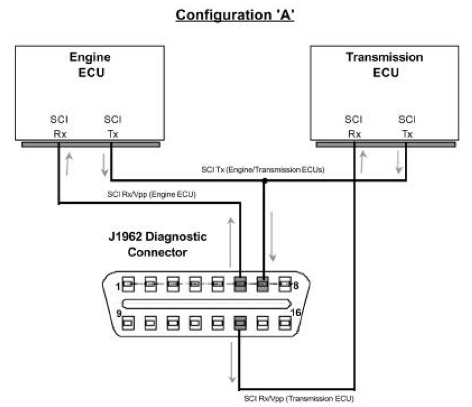
DIAGNOSTIC CONNECTOR MULTIPLEXING
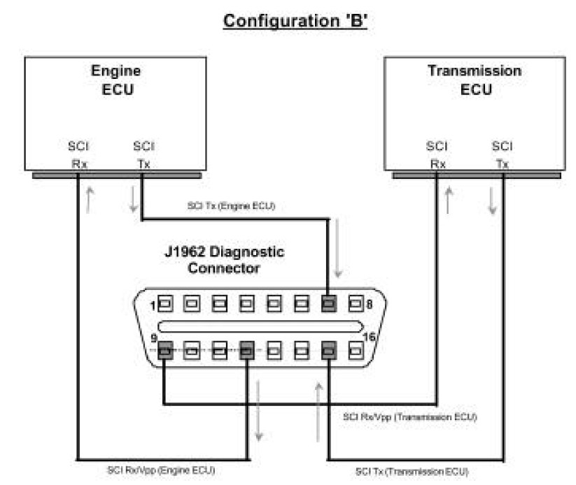
Multiplexing of the SAE J1962 diagnostic connector terminals shall be required by the diagnostic tester to support the two vehicle configurations as follows:
a. Configuration 'A'—For Configuration 'A', connector pins 6 and 14 shall be multiplexed between SCI functionality and ISO 15765-4 CAN functionality under software control.
SCI connections to pins 6 and 14 shall not electrically interfere with ISO 15765-4 CAN operation. Both pins must transition simultaneously between data link types when requested.
When the SCI mode is selected by the tester, both pins 6 and 14 must support SCI transmit with Vpp flash strobe function under software control.
The default settings for the SCI channel function are 7812.5 bps with flash strobe 'OFF'.
Connector pin 7 shall function as either an SCI receiver, or an ISO 9141-2 bi-directional transceiver under software control.
SCI connections to pin 7 shall not electrically interfere with ISO 9141-2 operations, and shall be able to be pulled to either vehicle battery or 5 V DC under programmable control.
b. Configuration 'B'—For Configuration 'B', connector pins 9 and 12 shall be configured for SCI functionality.
When the SCI mode is selected by the tester, both pins 9 and 12 must support SCI transmit with Vpp flash strobe function under software control.
Either connector pin transitions independently with SCI mode enabled.
The default settings for the SCI channel function are 7812.5bps with flash strobe 'OFF'.
Connector pins 7 and 15 shall function as either an SCI receiver, or an ISO 9141-2 transceiver under software control.
SCI connections to pins 7 or 15 shall not electrically interfere with ISO 9141-2 operations, and shall be able to be pulled to either vehicle battery or 5 V DC under programmable control.
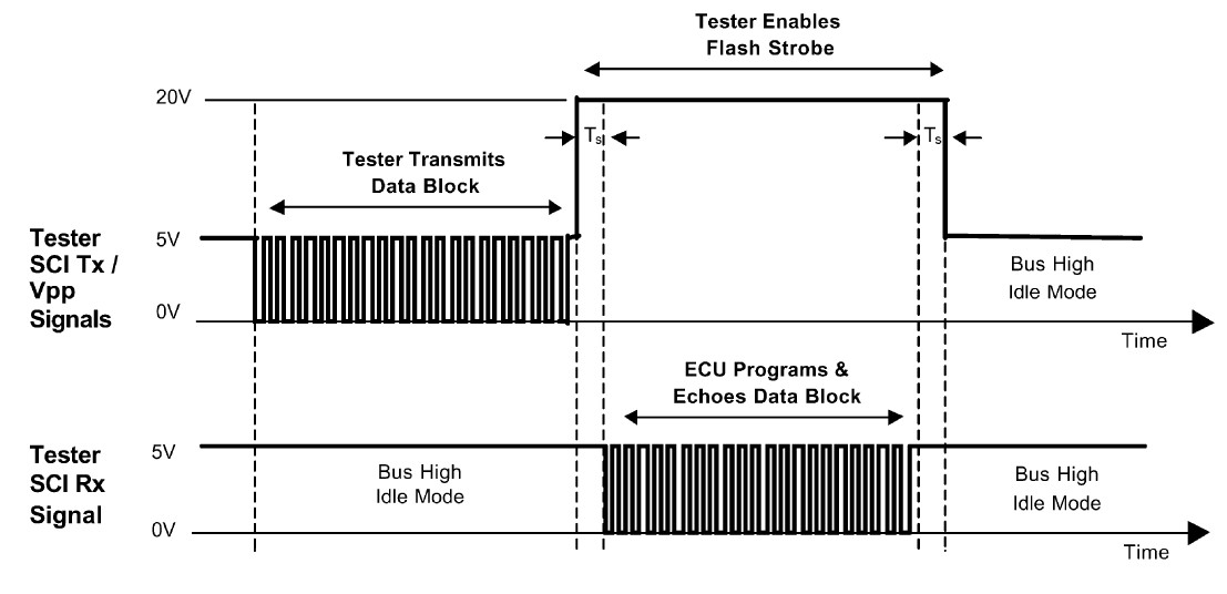
For additional details regarding the multiplexing of the Vpp flash strobe requirements during a flash reprogramming session, please refer to Section 9 “Reprogramming Requirements”.
ECU Receiver/Transmitter Reference Circuits—The following figures depict functionally equivalent SCI receive and transmit circuits for an ECU.
SCI RX LINE—The ECU receive circuit shall contain provisions to support SCI communications as well as Vpp flash strobe requirements multiplexed on the same line by the diagnostic tester.
A typical ECU receive circuit is shown
REPRESENTATIVE ECU RECEIVER CIRCUIT WITH TYPICAL COMPONENT VALUES
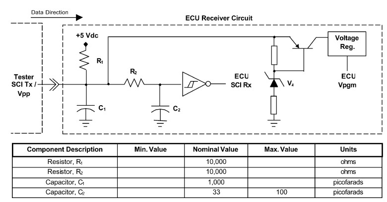
SCI TX LINE—The ECU transmit circuit shall contain an open-collector style circuit to drive a diagnostic tester receive circuit such as the one illustrated in Figure
The tester must provide adequate pull-up resistance as shown.

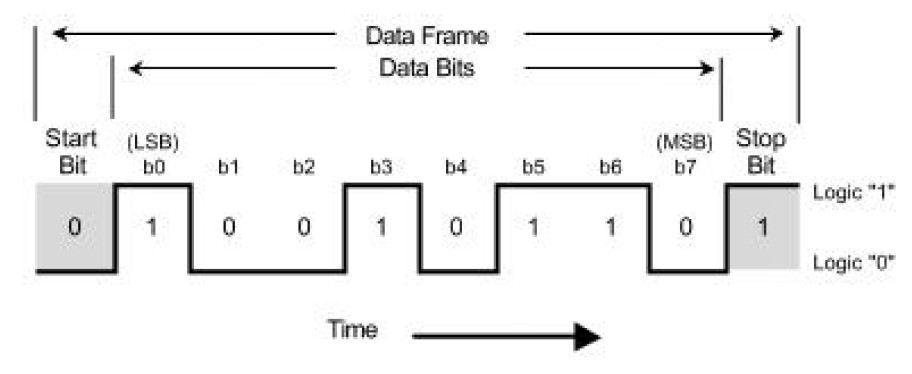
Data Frame Definition
Asynchronous data transmission implies that each data frame shall be transmitted individually.
This section defines the grouping of data bits that comprise an SCI data frame.
A data frame is defined as one complete transmission of information delineated by the start of frame (start bit) and end of frame (stop bit) identifiers.
These start and stop bits define the boundaries of a single data frame for the receiver to properly interpret.
LENGTH AND FORMAT
The data frame size shall be defined as ten (10) bits in length (i.e., one start bit, eight data bits, and one stop bit with no parity).
The format of the data frame shall be defined as follows:
a. One (1) Start Bit:One start bit with logic “0” (low) for one bit time duration.
The start bit is defined as the first binary element transmitted in the asynchronous transmission of a data frame.
It is used to uniquely identify the beginning of a data frame transmission to synchronize the receiver to an active session.
b. Eight (8) Data Bits:Eight data bits transmitted from Least Significant Bit (LSB) to Most Significant Bit (MSB).
The data bits comprise the byte or character value contained in the data frame bounded by the start and stop bits.
c. One (1) Stop Bit:One stop bit with logic “1” (high) for one bit time duration.
The stop bit is defined as the last binary element transmitted in the asynchronous transmission of a data frame.
It is used to uniquely identify the end of a data frame transmission to return the receiver to an idle condition.
d. No Parity Bit:No parity bit in the default data frame. Therefore, no parity checking is available in the transmitted data frame.
SCI/VPP MULTIPLEXING
Ford Networks
Ford Network Specifications:
- Standard Corporate Protocol – SCP
- J1850 PWM – 41.6k Dual Wire is used for OE Data transfer – Pins 2 & 10 – 5v
- J1850 VPW – 10.4k Single wire used for Global OBD II – Pin 2 only – 7 volts
- UBP – Universal Bus Protocol, a UART based network, typically found pre OBDII
Ford SCP
Ford’s variation of J-1850 is called Standard Corporate Protocol or SCP.
SCP uses a two wire twisted pair bus and is the most common network protocol used on late model Ford passenger vehicles.
The signal has a 0-5 volt toggle and the SCP+ and SCP- signals are mirrored. Take a look at the signals below.
Ford SCP Fault tolerances:
- An open on one wire should not affect bus communications
- However, a short to ground will cause a loss of communication to the scan tool
- A short to power will result in a dead bus

 浙公网安备 33010602011771号