


(原創) 如何以32 bit的方式存取SDRAM? (SOC) (Nios II) (SOPC Builder) (DE2-70)
 在DE2因為只有一顆16 bit的SDRAM,儘管Nios II CPU是32 bit,存取SDRAM時必須透過Dyanamic Bus Sizing機制,花2個clk才能將32 bit資料讀取/寫入SDRAM;但DE2-70有2顆16 bit SDRAM,是否能將這2顆16 bit SDRAM看成1顆32 bit SDRAM使用呢?
Abstract
在DE2因為只有一顆16 bit的SDRAM,儘管Nios II CPU是32 bit,存取SDRAM時必須透過Dyanamic Bus Sizing機制,花2個clk才能將32 bit資料讀取/寫入SDRAM;但DE2-70有2顆16 bit SDRAM,是否使用雙通道的方式,將這2顆16 bit SDRAM看成1顆32 bit SDRAM使用呢?
Introduction
這個做法是Mithril所提供,感謝Mithril無私的分享,我只是加以整理。
使用環境:Quartus II 8.1 + DE2-70 (Cyclone II EP2C70F896C6N)
在(原創) 哪裡有DE2-70的Nios II reference design可以參考? (SOC) (DE2-70) (Nios II) (SOPC Builder)與DE2-70 CD中提供的範例,如DE2_70_NET、DE2_70_NIOS_DEVICE_LED、DE2_70_NIOS_HOST_MOUSE_VGA、DE2_70_SD_Card_Audio_Player中,都是使用2個16 bit SDRAM controller,各自對應到2顆SDRAM。
不過可惜的是,SDRAM Controller的Data width只有16 bit,而Nios II CPU與其他ip都是32 bit,由於Data width不同,Avalon bus會啟動Dynamic Bus Sizing機制,2個clk才能完成32 bit傳輸。

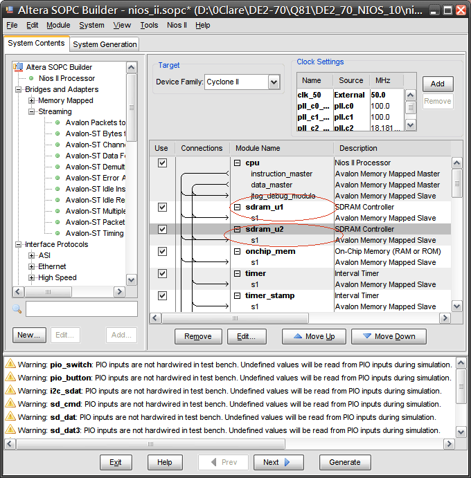
將2顆16 bit SDRAM當成1顆32 bit SDRAM使用
Step 1:
只留下1個SDRAM controller即可

Step 2:
Data width改成32 bit,其餘不用改

注意結果仍為64MB,顯然沒有因為只用了一個SDRAM controller而少抓memory size。
Step 3:
修改top module
DE2_70_NIOS.v / Verilog
2 (C) OOMusou 2008 http://oomusou.cnblogs.com
3
4 Filename : DE2_70_NIOS.v
5 Compiler : Quartus II 8.1
6 Description : DE2_70_NIOS reference design 1.1
7 Release : 11/25/2008 1.0
8 */
9
10 module DE2_70_NIOS (
11 input iCLK_28, // 28.63636 MHz
12 input iCLK_50, // 50 MHz
13 input iCLK_50_2, // 50 MHz
14 input iCLK_50_3, // 50 MHz
15 input iCLK_50_4, // 50 MHz
16 input iEXT_CLOCK, // External Clock
17 ////////////////////////////// Push Button ////////////////////////
18 input [3:0] iKEY, // Pushbutton[3:0]
19 ////////////////////////////// DPDT Switch ////////////////////////
20 input [17:0] iSW, // Toggle Switch[17:0]
21 ////////////////////////////// 7-SEG Dispaly ////////////////////////
22 output [6:0] oHEX0_D, // Seven Segment Digit 0
23 output oHEX0_DP, // Seven Segment Digit 0 decimal point
24 output [6:0] oHEX1_D, // Seven Segment Digit 1
25 output oHEX1_DP, // Seven Segment Digit 1 decimal point
26 output [6:0] oHEX2_D, // Seven Segment Digit 2
27 output oHEX2_DP, // Seven Segment Digit 2 decimal point
28 output [6:0] oHEX3_D, // Seven Segment Digit 3
29 output oHEX3_DP, // Seven Segment Digit 3 decimal point
30 output [6:0] oHEX4_D, // Seven Segment Digit 4
31 output oHEX4_DP, // Seven Segment Digit 4 decimal point
32 output [6:0] oHEX5_D, // Seven Segment Digit 5
33 output oHEX5_DP, // Seven Segment Digit 5 decimal point
34 output [6:0] oHEX6_D, // Seven Segment Digit 6
35 output oHEX6_DP, // Seven Segment Digit 6 decimal point
36 output [6:0] oHEX7_D, // Seven Segment Digit 7
37 output oHEX7_DP, // Seven Segment Digit 7 decimal point
38 //////////////////////////////// LED ////////////////////////////
39 output [8:0] oLEDG, // LED Green[8:0]
40 output [17:0] oLEDR, // LED Red[17:0]
41 //////////////////////////////// UART ////////////////////////////
42 output oUART_TXD, // UART Transmitter
43 input iUART_RXD, // UART Receiver
44 output oUART_CTS, // UART Clear To Send
45 input iUART_RTS, // UART Requst To Send
46 //////////////////////////////// IRDA ////////////////////////////
47 output oIRDA_TXD, // IRDA Transmitter
48 input iIRDA_RXD, // IRDA Receiver
49 //////////////////////////////// SDRAM Interface ////////////////////////
50 inout [31:0] DRAM_DQ, // SDRAM Data bus 32 Bits
51 output [12:0] oDRAM0_A, // SDRAM0 Address bus 12 Bits
52 output [12:0] oDRAM1_A, // SDRAM1 Address bus 12 Bits
53 output oDRAM0_LDQM0, // SDRAM0 Low-byte Data Mask
54 output oDRAM1_LDQM0, // SDRAM1 Low-byte Data Mask
55 output oDRAM0_UDQM1, // SDRAM0 High-byte Data Mask
56 output oDRAM1_UDQM1, // SDRAM1 High-byte Data Mask
57 output oDRAM0_WE_N, // SDRAM0 Write Enable
58 output oDRAM1_WE_N, // SDRAM1 Write Enable
59 output oDRAM0_CAS_N, // SDRAM0 Column Address Strobe
60 output oDRAM1_CAS_N, // SDRAM1 Column Address Strobe
61 output oDRAM0_RAS_N, // SDRAM0 Row Address Strobe
62 output oDRAM1_RAS_N, // SDRAM1 Row Address Strobe
63 output oDRAM0_CS_N, // SDRAM0 Chip Select
64 output oDRAM1_CS_N, // SDRAM1 Chip Select
65 output [1:0] oDRAM0_BA, // SDRAM0 Bank Address
66 output [1:0] oDRAM1_BA, // SDRAM1 Bank Address
67 output oDRAM0_CLK, // SDRAM0 Clock
68 output oDRAM1_CLK, // SDRAM0 Clock
69 output oDRAM0_CKE, // SDRAM0 Clock Enable
70 output oDRAM1_CKE, // SDRAM1 Clock Enable
71 //////////////////////////////// Flash Interface ////////////////////////
72 inout [14:0] FLASH_DQ, // FLASH Data bus 15 Bits (0 to 14)
73 inout FLASH_DQ15_AM1, // FLASH Data bus Bit 15 or Address A-1
74 output [25:0] oFLASH_A, // FLASH Address bus 26 Bits
75 output oFLASH_WE_N, // FLASH Write Enable
76 output oFLASH_RST_N, // FLASH Reset
77 output oFLASH_WP_N, // FLASH Write Protect /Programming Acceleration
78 input iFLASH_RY_N, // FLASH Ready/Busy output
79 output oFLASH_BYTE_N, // FLASH Byte/Word Mode Configuration
80 output oFLASH_OE_N, // FLASH Output Enable
81 output oFLASH_CE_N, // FLASH Chip Enable
82 //////////////////////////////// SRAM Interface ////////////////////////
83 inout [31:0] SRAM_DQ, // SRAM Data Bus 32 Bits
84 inout [3:0] SRAM_DPA, // SRAM Parity Data Bus
85 output [20:0] oSRAM_A, // SRAM Address bus 21 Bits
86 output oSRAM_ADSC_N, // RAM Controller Address Status
87 output oSRAM_ADSP_N, // SRAM Processor Address Status
88 output oSRAM_ADV_N, // SRAM Burst Address Advance
89 output [3:0] oSRAM_BE_N, // SRAM Byte Write Enable
90 output oSRAM_CE1_N, // SRAM Chip Enable
91 output oSRAM_CE2, // SRAM Chip Enable
92 output oSRAM_CE3_N, // SRAM Chip Enable
93 output oSRAM_CLK, // SRAM Clock
94 output oSRAM_GW_N, // SRAM Global Write Enable
95 output oSRAM_OE_N, // SRAM Output Enable
96 output oSRAM_WE_N, // SRAM Write Enable
97 //////////////////////////////// ISP1362 Interface ////////////////////////
98 inout [15:0] OTG_D, // ISP1362 Data bus 16 Bits
99 output [1:0] oOTG_A, // ISP1362 Address 2 Bits
100 output oOTG_CS_N, // ISP1362 Chip Select
101 output oOTG_OE_N, // ISP1362 Read
102 output oOTG_WE_N, // ISP1362 Write
103 output oOTG_RESET_N, // ISP1362 Reset
104 inout OTG_FSPEED, // USB Full Speed, 0 = Enable, Z = Disable
105 inout OTG_LSPEED, // USB Low Speed, 0 = Enable, Z = Disable
106 input iOTG_INT0, // ISP1362 Interrupt 0
107 input iOTG_INT1, // ISP1362 Interrupt 1
108 input iOTG_DREQ0, // ISP1362 DMA Request 0
109 input iOTG_DREQ1, // ISP1362 DMA Request 1
110 output oOTG_DACK0_N, // ISP1362 DMA Acknowledge 0
111 output oOTG_DACK1_N, // ISP1362 DMA Acknowledge 1
112 //////////////////////////////// LCD Module 16X2 ////////////////////////////
113 inout [7:0] LCD_D, // LCD Data bus 8 bits
114 output oLCD_ON, // LCD Power ON/OFF
115 output oLCD_BLON, // LCD Back Light ON/OFF
116 output oLCD_RW, // LCD Read/Write Select, 0 = Write, 1 = Read
117 output oLCD_EN, // LCD Enable
118 output oLCD_RS, // LCD Command/Data Select, 0 = Command, 1 = Data
119 //////////////////////////////// SD Card Interface ////////////////////////
120 inout SD_DAT, // SD Card Data
121 inout SD_DAT3, // SD Card Data 3
122 inout SD_CMD, // SD Card Command Signal
123 output oSD_CLK, // SD Card Clock
124 //////////////////////////////// I2C ////////////////////////////////
125 inout I2C_SDAT, // I2C Data
126 output oI2C_SCLK, // I2C Clock
127 //////////////////////////////// PS2 ////////////////////////////
128 inout PS2_KBDAT, // PS2 Keyboard Data
129 inout PS2_KBCLK, // PS2 Keyboard Clock
130 inout PS2_MSDAT, // PS2 Mouse Data
131 inout PS2_MSCLK, // PS2 Mouse Clock
132 //////////////////////////////// VGA ////////////////////////////
133 output oVGA_CLOCK, // VGA Clock
134 output oVGA_HS, // VGA H_SYNC
135 output oVGA_VS, // VGA V_SYNC
136 output oVGA_BLANK_N, // VGA BLANK
137 output oVGA_SYNC_N, // VGA SYNC
138 output [9:0] oVGA_R, // VGA Red[9:0]
139 output [9:0] oVGA_G, // VGA Green[9:0]
140 output [9:0] oVGA_B, // VGA Blue[9:0]
141 //////////////////////////////// Ethernet Interface ////////////////////////////
142 inout [15:0] ENET_D, // DM9000A DATA bus 16Bits
143 output oENET_CMD, // DM9000A Command/Data Select, 0 = Command, 1 = Data
144 output oENET_CS_N, // DM9000A Chip Select
145 output oENET_IOW_N, // DM9000A Write
146 output oENET_IOR_N, // DM9000A Read
147 output oENET_RESET_N, // DM9000A Reset
148 input iENET_INT, // DM9000A Interrupt
149 output oENET_CLK, // DM9000A Clock 25 MHz
150 //////////////////////////////// Audio CODEC ////////////////////////////
151 inout AUD_ADCLRCK, // Audio CODEC ADC LR Clock
152 input iAUD_ADCDAT, // Audio CODEC ADC Data
153 inout AUD_DACLRCK, // Audio CODEC DAC LR Clock
154 output oAUD_DACDAT, // Audio CODEC DAC Data
155 inout AUD_BCLK, // Audio CODEC Bit-Stream Clock
156 output oAUD_XCK, // Audio CODEC Chip Clock
157 //////////////////////////////// TV Devoder ////////////////////////////
158 input iTD1_CLK27, // TV Decoder1 Line_Lock Output Clock
159 input [7:0] iTD1_D, // TV Decoder1 Data bus 8 bits
160 input iTD1_HS, // TV Decoder1 H_SYNC
161 input iTD1_VS, // TV Decoder1 V_SYNC
162 output oTD1_RESET_N, // TV Decoder1 Reset
163 input iTD2_CLK27, // TV Decoder2 Line_Lock Output Clock
164 input [7:0] iTD2_D, // TV Decoder2 Data bus 8 bits
165 input iTD2_HS, // TV Decoder2 H_SYNC
166 input iTD2_VS, // TV Decoder2 V_SYNC
167 output oTD2_RESET_N, // TV Decoder2 Reset
168 //////////////////////////////// GPIO ////////////////////////////////
169 inout [31:0] GPIO_0, // GPIO Connection 0 I/O
170 input GPIO_CLKIN_N0, // GPIO Connection 0 Clock Input 0
171 input GPIO_CLKIN_P0, // GPIO Connection 0 Clock Input 1
172 output GPIO_CLKOUT_N0, // GPIO Connection 0 Clock Output 0
173 output GPIO_CLKOUT_P0, // GPIO Connection 0 Clock Output 1
174 inout [31:0] GPIO_1, // GPIO Connection 1 I/O
175 input GPIO_CLKIN_N1, // GPIO Connection 1 Clock Input 0
176 input GPIO_CLKIN_P1, // GPIO Connection 1 Clock Input 1
177 output GPIO_CLKOUT_N1, // GPIO Connection 1 Clock Output 0
178 output GPIO_CLKOUT_P1 // PIO Connection 1 Clock Output 1
179 );
180
181 // All inout port turn to tri-state
182 assign SD_DAT = 1'bz;
183 assign GPIO_0 = 32'hzzzzzzzzz;
184 assign GPIO_1 = 32'hzzzzzzzzz;
185 assign AUD_ADCLRCK = 1'bz;
186
187 // Turn On TV Decoder
188 assign oTD1_RESET_N = 1'bz;
189 assign oTD2_RESET_N = 1'bz;
190
191 // Flash
192 assign FL_RST_N = 1'b1;
193
194 // 16*2 LCD Module
195 assign oLCD_ON = 1'b1; // LCD ON
196 assign oLCD_BLON = 1'b1; // LCD Back Light
197
198 // Disable USB speed select
199 assign OTG_FSPEED = 1'bz;
200 assign OTG_LSPEED = 1'bz;
201
202 // FLASH
203 wire FLASH_16BIT_IP_A0;
204 assign oFLASH_BYTE_N = 1'b1; // FLASH Byte/Word Mode Configuration
205 assign oFLASH_RST_N = 1'b1; // FLASH Reset
206 assign oFLASH_WP_N = 1'b1; // FLASH Write Protect /Programming Acceleration
207
208 // SSRAM
209 wire SRAM_CLK;
210 wire [1:0] SRAM_DUMMY_ADDR; // used to ignore the A0/A1 pin from Cypress SSRAM IP core
211
212 assign oSRAM_ADSP_N = 1'b1; // SRAM Processor Address Status
213 assign oSRAM_ADV_N = 1'b1; // SRAM Burst Address Advance
214 assign oSRAM_CE2 = ~oSRAM_CE1_N; // SRAM Chip Enable
215 assign oSRAM_CE3_N = oSRAM_CE1_N; // SRAM Chip Enable
216 assign oSRAM_GW_N = 1'b1; // SRAM Global Write Enable
217 assign oSRAM_CLK = SRAM_CLK;
218
219 // SDRAM
220 // the sdram is shahred with rtl and nios
221 wire [12:0] dram_a;
222 wire [1:0] dram_ba;
223 wire dram_cas_n;
224 wire dram_cke;
225 wire dram_cs_n;
226 wire [3:0] dram_dqm;
227 wire dram_ras_n;
228 wire dram_we_n;
229
230 // dram1
231 assign oDRAM0_CLK = SRAM_CLK; // SDRAM0 Clock
232 assign oDRAM1_CLK = SRAM_CLK; // SDRAM1 Clock
233
234 assign oDRAM0_A = dram_a;
235 assign oDRAM0_BA = dram_ba;
236 assign oDRAM0_CAS_N = dram_cas_n;
237 assign oDRAM0_CKE = dram_cke;
238 assign oDRAM0_CS_N = dram_cs_n;
239 assign oDRAM0_LDQM0 = dram_dqm[0];
240 assign oDRAM0_UDQM1 = dram_dqm[1];
241 assign oDRAM0_RAS_N = dram_ras_n;
242 assign oDRAM0_WE_N = dram_we_n;
243
244 // dram2
245 assign oDRAM1_A = dram_a;
246 assign oDRAM1_BA = dram_ba;
247 assign oDRAM1_CAS_N = dram_cas_n;
248 assign oDRAM1_CKE = dram_cke;
249 assign oDRAM1_CS_N = dram_cs_n;
250 assign oDRAM1_LDQM0 = dram_dqm[2];
251 assign oDRAM1_UDQM1 = dram_dqm[3];
252 assign oDRAM1_RAS_N = dram_ras_n;
253 assign oDRAM1_WE_N = dram_we_n;
254
255 // USB
256 assign OTG_FSPEED = 1'bz; // USB Full Speed, 0 = Enable, Z = Disable
257 assign OTG_LSPEED = 1'bz; // USB Low Speed, 0 = Enable, Z = Disable
258
259 // Clock 25MHz
260 reg iCLK_25;
261
262 always@(posedge iCLK_50)
263 iCLK_25 <= ~iCLK_25;
264
265 // NIOS CPU
266 wire CPU_CLK;
267 wire CPU_RESET_N;
268
269 Reset_Delay delay0 (
270 .iRST(iKEY[0]),
271 .iCLK(iCLK_50),
272 .oRESET(CPU_RESET_N)
273 );
274
275 // NIOS II system
276 nios_ii nios_ii0 (
277 // 1) global signals:
278 .clk_50(iCLK_50),
279 .pll_c0_system(CPU_CLK),
280 .pll_c1_memory(SRAM_CLK),
281 .pll_c2_audio(oAUD_XCK),
282 .reset_n(CPU_RESET_N),
283 .clk_25(iCLK_25),
284 // the_DM9000A_IF_0
285 .avs_s1_export_ENET_CLK_from_the_DM9000A(oENET_CLK),
286 .avs_s1_export_ENET_CMD_from_the_DM9000A(oENET_CMD),
287 .avs_s1_export_ENET_CS_N_from_the_DM9000A(oENET_CS_N),
288 .avs_s1_export_ENET_DATA_to_and_from_the_DM9000A(ENET_D),
289 .avs_s1_export_ENET_INT_to_the_DM9000A(iENET_INT),
290 .avs_s1_export_ENET_RD_N_from_the_DM9000A(oENET_IOR_N),
291 .avs_s1_export_ENET_RST_N_from_the_DM9000A(oENET_RESET_N),
292 .avs_s1_export_ENET_WR_N_from_the_DM9000A(oENET_IOW_N),
293 // the_ISP1362
294 .avs_hc_export_OTG_ADDR_from_the_ISP1362(oOTG_A),
295 .avs_hc_export_OTG_CS_N_from_the_ISP1362(oOTG_CS_N),
296 .avs_hc_export_OTG_DATA_to_and_from_the_ISP1362(OTG_D),
297 .avs_hc_export_OTG_INT0_to_the_ISP1362(iOTG_INT0),
298 .avs_hc_export_OTG_RD_N_from_the_ISP1362(oOTG_OE_N),
299 .avs_hc_export_OTG_RST_N_from_the_ISP1362(oOTG_RESET_N),
300 .avs_hc_export_OTG_WR_N_from_the_ISP1362(oOTG_WE_N),
301 .avs_dc_export_OTG_INT1_to_the_ISP1362(iOTG_INT1),
302 // the_audio
303 .avs_s1_export_BCLK_to_the_AUDIO(AUD_BCLK),
304 .avs_s1_export_DACLRC_to_the_AUDIO(AUD_DACLRCK),
305 .avs_s1_export_DACDAT_from_the_AUDIO(oAUD_DACDAT),
306 .avs_s1_export_ADCLRC_to_the_AUDIO(AUD_ADCLRCK),
307 .avs_s1_export_ADCDAT_to_the_AUDIO(iAUD_ADCDAT),
308 // the_i2c_sclk
309 .out_port_from_the_i2c_sclk(oI2C_SCLK),
310 // the_i2c_sdat
311 .bidir_port_to_and_from_the_i2c_sdat(I2C_SDAT),
312 // the_lcd
313 .LCD_E_from_the_lcd(oLCD_EN),
314 .LCD_RS_from_the_lcd(oLCD_RS),
315 .LCD_RW_from_the_lcd(oLCD_RW),
316 .LCD_data_to_and_from_the_lcd(LCD_D),
317 // the_pio_button
318 .in_port_to_the_pio_button(iKEY),
319 // the_pio_green_led
320 .out_port_from_the_pio_green_led(oLEDG),
321 // the_pio_red_led
322 .out_port_from_the_pio_red_led(oLEDR),
323 // the_seg7
324 .avs_s1_export_seg7_from_the_SEG7({oHEX7_DP, oHEX7_D, oHEX6_DP, oHEX6_D, oHEX5_DP,
325 oHEX5_D, oHEX4_DP,oHEX4_D, oHEX3_DP, oHEX3_D, oHEX2_DP, oHEX2_D, oHEX1_DP, oHEX1_D,
326 oHEX0_DP, oHEX0_D}),
327 // the_pio_switch
328 .in_port_to_the_pio_switch(iSW),
329 // the_sd_clk
330 .out_port_from_the_sd_clk(oSD_CLK),
331 // the_sd_cmd
332 .bidir_port_to_and_from_the_sd_cmd(SD_CMD),
333 // the_sd_dat
334 .bidir_port_to_and_from_the_sd_dat(SD_DAT),
335 // the_sd_dat3
336 .bidir_port_to_and_from_the_sd_dat3(SD_DAT3),
337 // the_sdram (u1)
338 .zs_addr_from_the_sdram_u1(dram_a),
339 .zs_ba_from_the_sdram_u1(dram_ba),
340 .zs_cas_n_from_the_sdram_u1(dram_cas_n),
341 .zs_cke_from_the_sdram_u1(dram_cke),
342 .zs_cs_n_from_the_sdram_u1(dram_cs_n),
343 .zs_dq_to_and_from_the_sdram_u1(DRAM_DQ),
344 .zs_dqm_from_the_sdram_u1(dram_dqm),
345 .zs_ras_n_from_the_sdram_u1(dram_ras_n),
346 .zs_we_n_from_the_sdram_u1(dram_we_n),
347 // the_tristate_bridge_avalon_slave (flash)
348 .address_to_the_cfi_flash({oFLASH_A[21:0],FLASH_16BIT_IP_A0}),
349 .data_to_and_from_the_cfi_flash({FLASH_DQ15_AM1,FLASH_DQ}),
350 .read_n_to_the_cfi_flash(oFLASH_OE_N),
351 .select_n_to_the_cfi_flash(oFLASH_CE_N),
352 .write_n_to_the_cfi_flash(oFLASH_WE_N),
353 // the_tristate_bridge_1_avalon_slave (ssram)
354 .address_to_the_ssram({oSRAM_A[17:0],SRAM_DUMMY_ADDR}),
355 .adsc_n_to_the_ssram(oSRAM_ADSC_N),
356 .bw_n_to_the_ssram(oSRAM_BE_N),
357 .bwe_n_to_the_ssram(oSRAM_WE_N),
358 .chipenable1_n_to_the_ssram(oSRAM_CE1_N),
359 .data_to_and_from_the_ssram((SRAM_DQ)),
360 .outputenable_n_to_the_ssram(oSRAM_OE_N),
361 // the_uart
362 .cts_n_to_the_uart(oUART_CTS),
363 .rts_n_from_the_uart(iUART_RTS),
364 .rxd_to_the_uart(iUART_RXD),
365 .txd_from_the_uart(oUART_TXD),
366 );
367
368 endmodule
219行
// the sdram is shahred with rtl and nios
wire [12:0] dram_a;
wire [1:0] dram_ba;
wire dram_cas_n;
wire dram_cke;
wire dram_cs_n;
wire [3:0] dram_dqm;
wire dram_ras_n;
wire dram_we_n;
// dram1
assign oDRAM0_CLK = SRAM_CLK; // SDRAM0 Clock
assign oDRAM1_CLK = SRAM_CLK; // SDRAM1 Clock
assign oDRAM0_A = dram_a;
assign oDRAM0_BA = dram_ba;
assign oDRAM0_CAS_N = dram_cas_n;
assign oDRAM0_CKE = dram_cke;
assign oDRAM0_CS_N = dram_cs_n;
assign oDRAM0_LDQM0 = dram_dqm[0];
assign oDRAM0_UDQM1 = dram_dqm[1];
assign oDRAM0_RAS_N = dram_ras_n;
assign oDRAM0_WE_N = dram_we_n;
// dram2
assign oDRAM1_A = dram_a;
assign oDRAM1_BA = dram_ba;
assign oDRAM1_CAS_N = dram_cas_n;
assign oDRAM1_CKE = dram_cke;
assign oDRAM1_CS_N = dram_cs_n;
assign oDRAM1_LDQM0 = dram_dqm[2];
assign oDRAM1_UDQM1 = dram_dqm[3];
assign oDRAM1_RAS_N = dram_ras_n;
assign oDRAM1_WE_N = dram_we_n;
宣告從SOPC的SDRAM port所連出的wire,並且連到top module的SDRAM port。
關鍵在於DRAM_DQ是個inout [31:0],不能設成wire,必須要直接從SOPC接出來,我第一次就是這樣失敗的。
337行
.zs_addr_from_the_sdram_u1(dram_a),
.zs_ba_from_the_sdram_u1(dram_ba),
.zs_cas_n_from_the_sdram_u1(dram_cas_n),
.zs_cke_from_the_sdram_u1(dram_cke),
.zs_cs_n_from_the_sdram_u1(dram_cs_n),
.zs_dq_to_and_from_the_sdram_u1(DRAM_DQ),
.zs_dqm_from_the_sdram_u1(dram_dqm),
.zs_ras_n_from_the_sdram_u1(dram_ras_n),
.zs_we_n_from_the_sdram_u1(dram_we_n),
從SOPC的SDRAM port連出的wire。
證明這種方式的正確性
從三個方式來證明:
1.執行Hello World project template,並將Nios II程式跑在SDRAM上。
2.執行Hello MicroC/OS-II project template,並將Nios II程式跑在SDRAM上。
3.執行Memory Test project template,證明64MB SDRAM皆可正常存取。
1.Hello World

執行結果

2.Hello MicroC/OS-II

執行結果

3.Memory Test
儘管能順利的在SDRAM執行Hello World與Hello MicroC/OS-II,還是很令人擔心這種方式是否能正確的存取DE2-70的64MB SDRAM,為了客觀起見,我們使用了Nios II內建的Memory Test project template。
Step 1:
使用Memory Test project template

Step 2:
將Nios II跑在SSRAM
因為SDRAM即將接受測試,所以將Nios II程式跑在SSRAM上

Step 3:
執行Memory Test

因為要測試SDRAM,所以輸入a繼續。

接著要我們輸入要測試的memory起始位置與結束位置,該怎麼填呢?回想一下SOPC Builder怎麼對SDRAM定址。

根據SOPC Builder,0x04000000為SDRAM的起始位置,0x07ffffff為結束位置。
執行結果

證明64MB SDRAM通過測試。
完整程式碼下載
DE2_70_NIOS_11.7z
Conclusion
或許有些人喜歡將2顆SDRAM分開使用,甚至有人1顆SDRAM是掛在Avalon bus上,另外1顆直接使用Sdram_Control_4Port控制;這就類似有人喜歡一顆硬碟分割成好幾個磁區,也有人喜歡將好幾顆硬碟合併成一顆使用。不過以傳輸來說,既然Nios II CPU是32 bit,所有的ip都是32 bit,SDRAM的16 bit反而是傳輸上的瓶頸,透過本文雙通道的方式,將2顆16 bit SDRAM合併成1顆32 bit SDRAM使用,可以讓整個系統順暢的以32 bit運行,不再需要Avalon bus的Dynamic Bus Sizing機制,充分發揮DE2-70兩顆SDRAM的優勢。
See Also
(原創) 哪裡有DE2-70的Nios II reference design可以參考? (SOC) (DE2-70) (Nios II) (SOPC Builder)
(原創) avm_m1_writedata[15:0] 與 avm_m1_writedata[31:0]配合avm_m1_byteenable = 4'b0011意義是否一樣? (SOC) (SOPC Builder) (DE2-70)
(原創) 如何使用Pipeline Bridge增進Nios II系統的Fmax? (SOC) (Quartus II) (Nios II) (SOPC Builder) (DE2-70)

 浙公网安备 33010602011771号