
如何为编程爱好者设计一款好玩的智能硬件(十)——无线2.4G通信模块研究·一篇说完
六、温湿度传感器DHT11驱动封装(下):如何为编程爱好者设计一款好玩的智能硬件(六)——初尝试·把温湿度给收集了(下)!
七、点阵字符型液晶显示模块LCD1602驱动封装(上):如何为编程爱好者设计一款好玩的智能硬件(七)——LCD1602点阵字符型液晶显示模块驱动封装(上)
八、LCD1602点阵字符型液晶显示模块驱动封装(中):如何为编程爱好者设计一款好玩的智能硬件(八)——LCD1602点阵字符型液晶显示模块驱动封装(中)
九、LCD1602点阵字符型液晶显示模块驱动封装(下):如何为编程爱好者设计一款好玩的智能硬件(九)——LCD1602点阵字符型液晶显示模块驱动封装(下)
十、nRF24L01无线2.4G一篇说完
承接上文,本节将从零开始带你认识无线2.4G模块,了解其控制和通信指令,从而封装一个nRF24L01底层的驱动函数,并最终写一个3-3通信的小实验验证我们的封装。在Quick Know部分你将快速浏览到nRF24L01的基本信息;在Thorough Understand部分你将深入nRF24L01细节了解其通信属性;在最后一部分你将看到我关于nRF24L01的底层驱动封装,并基于这个封装做了个简陋的3对3无线互传实验。
QUICK KNOW
1、芯片简介:
NRF24L01 是 NORDIC 公司最近生产的一款无线通信通信芯片,采用 FSK 调制,内部集成 NORDIC 自己的 Enhanced Short Burst 协议。可以实现点对点或是 1 对 6 的无线通信。无线通信速度可以达到 2M(bps)。NORDIC 公司提供通信模块的 GERBER 文件,可以直接加工生产。嵌入式工程师或是单片机爱好者只需要为单片机系统预留 5 个GPIO,1 个中断输入引脚,就可以很容易实现无线通信的功能,非常适合用来为 MCU 系统构建无线通信功能。
2、数据接口主要是SPI接口:
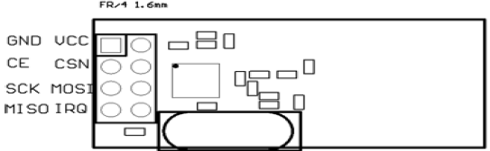
CSN:芯片的片选线,CSN 为低电平芯片工作。
SCK:芯片控制的时钟线(SPI 时钟)
MISO:芯片控制数据线(Master input slave output)
MOSI:芯片控制数据线(Master output slave input)
IRQ:中断信号。无线通信过程中 MCU 主要是通过 IRQ 与 NRF24L01 进行通信。
CE: 芯片的模式控制线。在 CSN 为低的情况下,CE 协同 NRF24L01 的 CONFIG 寄存器共同决定 NRF24L01 的状态(参照 NRF24L01 的状态机)。
3、NRF24L01状态及状态机:
Power Down Mode:掉电模式
Tx Mode:发射模式
Rx Mode:接收模式
Standby-1 Mode:待机 1 模式
Standby-2 Mode:待机 2 模式
4、对24L01的固件编程的基本思路如下:
5、Tx与Rx的配置过程 :
Tx模式初始化过程
| 1)写 Tx 节点的地址 | TX_ADDR |
| 2)写 Rx 节点的地址(主要是为了使能 Auto Ack) | RX_ADDR_P0 |
| 3)使能 AUTO ACK | EN_AA |
| 4)使能 PIPE 0 | EN_RXADDR |
| 5)配置自动重发次数 | SETUP_RETR |
| 6)选择通信频率 | RF_CH |
| 7)配置发射参数(低噪放大器增益、发射功率、无线速率) | RF_SETUP |
| 8 ) 选择通道 0 有效数据宽度 | Rx_Pw_P0 |
| 9)配置 24L01 的基本参数以及切换工作模式 | CONFIG |
Rx 模式初始化过程
| 1)写 Rx 节点的地址 | RX_ADDR_P0 |
| 2)使能 AUTO ACK | EN_AA |
| 3)使能 PIPE 0 | EN_RXADDR |
| 4)选择通信频率 | RF_CH |
| 5) 选择通道 0 有效数据宽度 | Rx_Pw_P0 |
| 6)配置发射参数(低噪放大器增益、发射功率、无线速率) | RF_SETUP |
| 7)配置 24L01 的基本参数以及切换工作模式 | CONFIG |
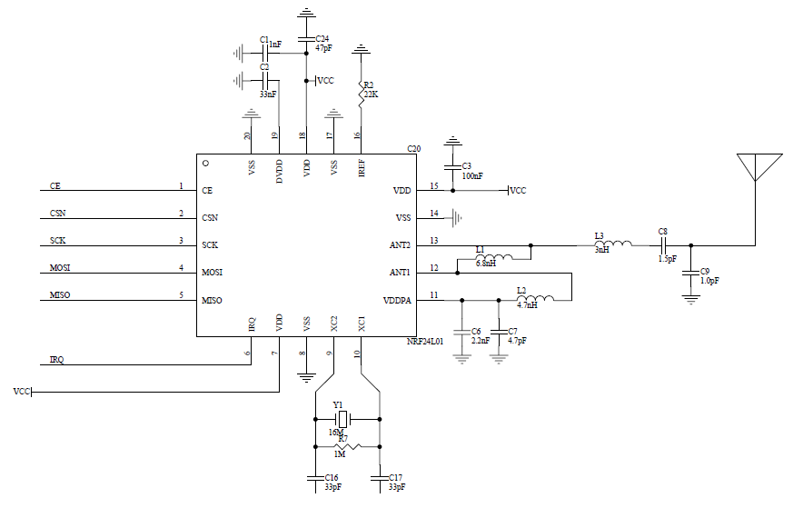
6、原理图:
THOROUGH UNDERSTAND
1、Introduction:
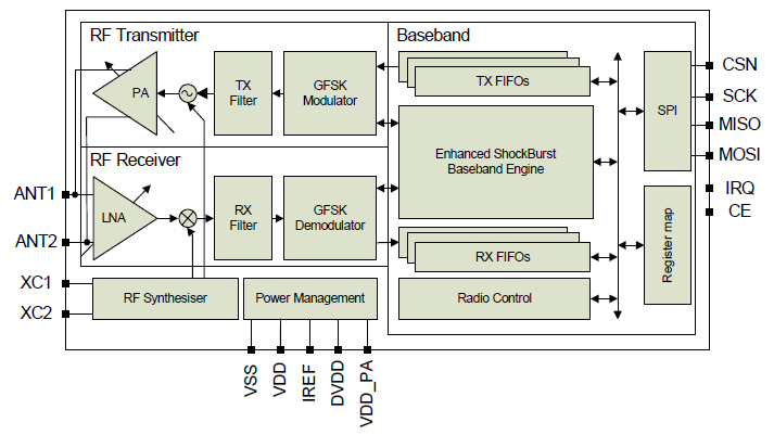
The nRF24L01+ is a single chip 2.4GHz transceiver with an embedded baseband protocol engine(Enhanced ShockBurst™), suitable for ultra low power wireless applications. The nRF24L01+ is designed for operation in the world wide ISM frequency band at 2.400 - 2.4835GHz.
To design a radio system with the nRF24L01+, you simply need an MCU (microcontroller) and a few external passive components.
You can operate and configure the nRF24L01+ through a Serial Peripheral Interface (SPI). The register map, which is accessible through the SPI, contains all configuration registers in the nRF24L01+ and is accessible in all operation modes of the chip.
The embedded baseband protocol engine (Enhanced ShockBurst™) is based on packet communication and supports various modes from manual operation to advanced autonomous protocol operation. Internal FIFOs ensure a smooth data flow between the radio front end and the system’s MCU. Enhanced Shock-Burst™ reduces system cost by handling all the high speed link layer operations.
The radio front end uses GFSK modulation. It has user configurable parameters like frequency channel,output power and air data rate. nRF24L01+ supports an air data rate of 250 kbps, 1 Mbps and 2Mbps. The high air data rate combined with two power saving modes make the nRF24L01+ very suitable for ultra low power designs.
nRF24L01+ is drop-in compatible with nRF24L01 and on-air compatible with nRF2401A, nRF2402,nRF24E1 and nRF24E2. Intermodulation and wideband blocking values in nRF24L01+ are much improved in comparison to the nRF24L01 and the addition of internal filtering to nRF24L01+ has improved the margins for meeting RF regulatory standards.
Internal voltage regulators ensure a high Power Supply Rejection Ratio (PSRR) and a wide power supply range.
2、Features:
• Radio
Worldwide 2.4GHz ISM band operation
126 RF channels
Common RX and TX interface
GFSK modulation
250kbps, 1 and 2Mbps air data rate
1MHz non-overlapping channel spacing at 1Mbps
2MHz non-overlapping channel spacing at 2Mbps
• Transmitter
Programmable output power: 0, -6, -12 or -18dBm
11.3mA at 0dBm output power
• Receiver
Fast AGC for improved dynamic range
Integrated channel filters
13.5mA at 2Mbps
-82dBm sensitivity at 2Mbps
-85dBm sensitivity at 1Mbps
-94dBm sensitivity at 250kbps
• RF Synthesizer
Fully integrated synthesizer
No external loop filer, VCO varactor diode or resonator
Accepts low cost ±60ppm 16MHz crystal
• Enhanced ShockBurst™
1 to 32 bytes dynamic payload length
Automatic packet handling
Auto packet transaction handling
6 data pipe MultiCeiver™ for 1:6 star networks
• Power Management
Integrated voltage regulator
1.9 to 3.6V supply range
Idle modes with fast start-up times for advanced power management
26μA Standby-I mode, 900nA power down mode
Max 1.5ms start-up from power down mode
Max 130us start-up from standby-I mode
• Host Interface
4-pin hardware SPI
Max 10Mbps
3 separate 32 bytes TX and RX FIFOs
5V tolerant inputs
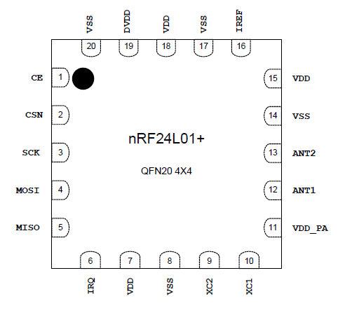
• Compact 20-pin 4x4mm QFN package
3、Operational Modes:
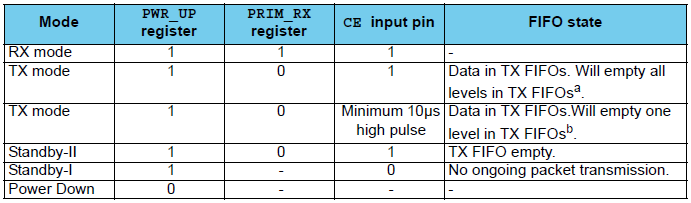
You can configure the nRF24L01+ in power down, standby, RX or TX mode. This section describes these modes in detail.

- Power Down Mode
In power down mode nRF24L01+ is disabled using minimal current consumption. All register values available are maintained and the SPI is kept active, enabling change of configuration and the uploading/downloading of data registers. Power down mode is entered by setting the PWR_UP bit in the CONFIG register low.
- Standby-I mode
By setting the PWR_UP bit in the CONFIG register to 1, the device enters standby-I mode. Standby-I mode is used to minimize average current consumption while maintaining short start up times. In this mode only part of the crystal oscillator is active. Change to active modes only happens if CE is set high and when CE is set low, the nRF24L01 returns to standby-I mode from both the TX and RX modes.
- Standby-II mode
In standby-II mode extra clock buffers are active and more current is used compared to standby-I mode. nRF24L01+ enters standby-II mode if CE is held high on a PTX device with an empty TX FIFO. If a new packet is uploaded to the TX FIFO, the PLL immediately starts and the packet is transmitted after the normal PLL settling delay (130μs).Register values are maintained and the SPI can be activated during both standby modes.
- RX mode(important one !!!)
The RX mode is an active mode where the nRF24L01+ radio is used as a receiver. To enter this mode, the nRF24L01+ must have the PWR_UP bit, PRIM_RX bit and the CE pin set high.
In RX mode the receiver demodulates the signals from the RF channel, constantly presenting the demodulated data to the baseband protocol engine. The baseband protocol engine constantly searches for a valid packet. If a valid packet is found (by a matching address and a valid CRC) the payload of the packet is presented in a vacant slot in the RX FIFOs. If the RX FIFOs are full, the received packet is discarded.
The nRF24L01+ remains in RX mode until the MCU configures it to standby-I mode or power down mode. However, if the automatic protocol features (Enhanced ShockBurst™) in the baseband protocol engine are enabled, the nRF24L01+ can enter other modes in order to execute the protocol.
In RX mode a Received Power Detector (RPD) signal is available. The RPD is a signal that is set high when a RF signal higher than -64 dBm is detected inside the receiving frequency channel. The internal RPD signal is filtered before presented to the RPD register. The RF signal must be present for at least 40μs before the RPD is set high.
- TX mode (also the important mode!!!)
The TX mode is an active mode for transmitting packets. To enter this mode, the nRF24L01+ must have the PWR_UP bit set high, PRIM_RX bit set low, a payload in the TX FIFO and a high pulse on the CE for more than 10μs.
The nRF24L01+ stays in TX mode until it finishes transmitting a packet. If CE = 0, nRF24L01+ returns to standby-I mode. If CE = 1, the status of the TX FIFO determines the next action. If the TX FIFO is not empty the nRF24L01+ remains in TX mode and transmits the next packet. If the TX FIFO is empty the nRF24L01+ goes into standby-II mode. The nRF24L01+ transmitter PLL operates in open loop when in TX mode. It is important never to keep the nRF24L01+ in TX mode for more than 4ms at a time. If the Enhanced ShockBurst™ features are enabled, nRF24L01+ is never in TX mode longer than 4ms.
The following table describes how to configure the operational modes
4、Air data rate:
The air data rate is the modulated signaling rate the nRF24L01+ uses when transmitting and receiving data. It can be 250kbps, 1Mbps or 2Mbps. Using lower air data rate gives better receiver sensitivity than higher air data rate. But, high air data rate gives lower average current consumption and reduced probability of on-air collisions.(high rate low right data transmission)
The air data rate is set by the RF_DR bit in the RF_SETUP register. A transmitter and a receiver must be programmed with the same air data rate to communicate with each other.
nRF24L01+ is fully compatible with nRF24L01. For compatibility with nRF2401A, nRF2402, nRF24E1, and nRF24E2 the air data rate must be set to 250kbps or 1Mbps.
5、RF channel frequency:
The RF channel frequency determines the center of the channel used by the nRF24L01+. The channel occupies a bandwidth of less than 1MHz at 250kbps and 1Mbps and a bandwidth of less than 2MHz at 2Mbps. nRF24L01+ can operate on frequencies from 2.400GHz to 2.525GHz. The programming resolution of the RF channel frequency setting is 1MHz.
At 2Mbps the channel occupies a bandwidth wider than the resolution of the RF channel frequency setting. To ensure non-overlapping channels in 2Mbps mode, the channel spacing must be 2MHz or more. At 1Mbps and 250kbps the channel bandwidth is the same or lower than the resolution of the RF frequency.
The RF channel frequency is set by the RF_CH register according to the following formula:
F0= 2400 + RF_CH [MHz]
You must program a transmitter and a receiver with the same RF channel frequency to communicate with each other.
6、数据包处理方式:
nRF24L01 有如下几种数据包处理方式
ShockBurstTM 与nRF2401 nRF24E1 nRF2402 nRF24E2 数据传输率为1Mbps 时相同
增强型ShockBurstTM 模式
7、ShockBurstTM 模式:
ShockBurst 模式下,nRF24L01可以与成本较低的低速MCU相连,高速信号处理是由芯片内部的射频协议处理的,nRF24L01提供SPI 接口数据率取决于单片机本身接口速度。ShockBurst 模式通过允许与单片机低速通信而无线部分高速通信,减小了通信的平均消耗电流。
在ShockBurstTM 接收模式下当接收到有效的地址和数据时,IRQ通知MCU,随后MCU可将接收到的数据从RX FIFO 寄存器中读出。
在ShockBurstTM 发送模式下,nRF24L01自动生成前导码及CRC。数据发送完毕后IRQ通知MCU,减少了MCU的查询时间,也就意味着减少了MCU 的工作量同时减少了软件的开发时间。nRF24L01 内部有三个不同的RX FIFO 寄存器,6 个通道共享此寄存器和三个不同的TX FIFO 寄存器。在掉电模式下、待机模式下和数据传输的过程中MCU 可以随时访问FIFO 寄存器,这就允许SPI接口可以以低速进行数据传送并且可以应用于MCU 硬件上没有SPI 接口的情况下。
8、增强型的ShockBurstTM 模式:
增强型 ShockBurstTM 模式可以使得双向链接协议执行起来更为容易、有效。典型的双向链接为发送方要求终端设备在接收到数据后有应答信号,以便于发送方检测有无数据丢失,一旦数据丢失则通过重
新发送功能将丢失的数据恢复。增强型的ShockBurstTM 模式可以同时控制应答及重发功能而无需增加MCU工作量。
9、MultiCeiver™:
MultiCeiver™ is a feature used in RX mode that contains a set of six parallel data pipes with unique addresses. A data pipe is a logical channel in the physical RF channel. Each data pipe has its own physical address (data pipe address) decoding in the nRF24L01+.
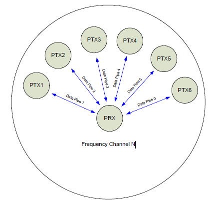
nRF24L01+ configured as PRX (primary receiver) can receive data addressed to six different data pipes in one frequency channel as shown in Figure up. Each data pipe has its own unique address and can be configured for individual behavior.
Up to six nRF24L01+s configured as PTX can communicate with one nRF24L01+ configured as a PRX. All data pipe addresses are searched for simultaneously(同时地). Only one data pipe can receive a packet at a time. All data pipes can perform Enhanced ShockBurst™ functionality.
The following settings are common to all data pipes:
• CRC enabled/disabled (CRC always enabled when Enhanced ShockBurst™ is enabled)
• CRC encoding scheme
• RX address width
• Frequency channel
• Air data rate
• LNA gain
注:The data pipes are enabled with the bits in the EN_RXADDR register. By default only data pipe 0 and 1 are enabled. Each data pipe address is configured in the RX_ADDR_PX registers.
注: Always ensure that none of the data pipes have the same address.
数据通道0是唯一的一个可以配置为40 位自身地址的数据通道1~5数据通道都为8位自身地址和32位公用地址。The LSByte must be unique for all six pipes. Flowing figure is an example of how data pipes 0-5 are addressed.
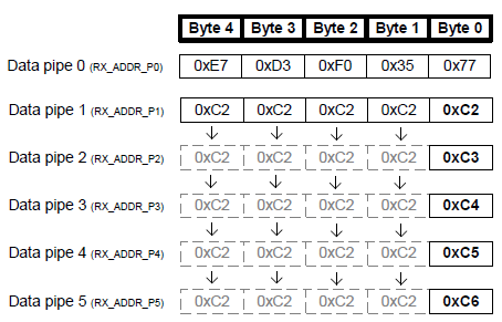
nRF24L01在确认收到数据后记录地址并以此地址为目标地址发送应答信号。在发送端数据通道0被用做接收应答信号,因此,数据通道0的接收地址要与发送端地址相等,以确保接收到正确的应答信号。
nRF24L01配置为增强型的ShockBurstTM发送模式下时,只要MCU有数据要发送nRF24L01就会启动ShockBurstTM模式来发送数据。在发送完数据后,nRF24L01转到接收模式并等待终端的应答信号。如果没有收到应答信号,nRF24L01将重发相同的数据包,直到收到应答信号或重发次数超过SETUP_RETR_ARC寄存器中设置的值为止(如果重发次数超过了设定值则产生MAX_RT中断)。只要收到确认信号,nRF24L01 就认为最后一包数据已经发送成功(接收方已经收到数据),把TX FIFO中的数据清除掉并产生TX_DS(中断IRQ引脚置高)。
START PROGRAMMING
上面看了那么多文字,想来头疼,遂!
最终效果视频
三个51单片机开发板每个都接一个无线2.4G模块
上位机通过串口向任何一个模块发送指令"1",该模块会向其他模块发送该信息
其他模块收到该信息则单片机控制一个灯闪烁表示收到数据
三个模块配置为发送地址和接收地址全部一样,所以可以互相通信
1、工程概览
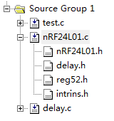
为了方便,这里的delay文件是借用前几次的(不要看)
2.4G模块封装全在nRF24L01.C和.H文件中(重点)
test.C文件中主要是main函数,实现通信逻辑(了解)
2、封装讲解
在.H中前面主要是对nRF24L01通信引脚(6个的宏定义-便于移植到其他平台),每个封装类似,如下:
1 #define nRF24L01_CE_PIN                        nRF24L01_CE
2 #define nRF24L01_CE_PIN_SET                nRF24L01_CE=1
3 #define nRF24L01_CE_PIN_CLEAR            nRF24L01_CE=0
4 //#define nRF24L01_CE_PIN_IN
5 //#define nRF24L01_CE_PIN_OUT
6 #define nRF24L01_CE_PIN_WRITE            nRF24L01_CE
7 #define nRF24L01_CE_PIN_READ            nRF24L01_CE
因为这几个引脚没有既是输出又要做输入的引脚,所以注释掉了第4、5两行,但是对于CC2541这样的单片机,虽然省了引脚属性切换,但是还是要在初始化的地方进行属性设置的!由于51的引脚操作简单,所以set、clear、read、write都比较简单。
接着是nRF24L01的一些寄存器指令和寄存器地址,这里只贴部分:
 1 //NRF24L01寄存器指令
 2 #define READ_REG        0x00      // 读寄存器指令
 3 #define WRITE_REG       0x20     // 写寄存器指令
 4 #define RD_RX_PLOAD     0x61      // 读取接收数据指令
 5 #define WR_TX_PLOAD     0xA0      // 写待发数据指令
 6 #define FLUSH_TX        0xE1     // 冲洗发送 FIFO指令
 7 #define FLUSH_RX        0xE2      // 冲洗接收 FIFO指令
 8 #define REUSE_TX_PL     0xE3      // 定义重复装载数据指令
 9 #define NOP             0xFF      // 保留
10 //SPI(nRF24L01)寄存器地址
11 #define CONFIG          0x00  // 配置收发状态,CRC校验模式以及收发状态响应方式
12 #define EN_AA           0x01  // 自动应答功能设置
13 #define EN_RXADDR       0x02  // 可用信道设置
14 #define SETUP_AW        0x03  // 收发地址宽度设置
15 #define SETUP_RETR      0x04  // 自动重发功能设置
最后是.C内封装的函数,上面几个是基本通信函数(其中第一个是最基本的通信函数,负责传送8bit数据)。下面几个就是nRF24L01的功能函数,分别负责初始化、检测是否正常、设置为接收模式、设置为发送模式、接收数据和发送数据。一会在main函数中你会看到一些关于它们的基本组合用法。
 1 t_uc nRF24L01_SPI_SendByte(t_uc dat);//传送一字节的超底层的通信函数
 2 t_uc nRF24L01_SPI_ReadReg(t_uc reg);//NRF24L01的SPI时序,读取指定寄存器的内容
 3 t_uc nRF24L01_SPI_WriteReg(t_uc reg, t_uc value);//NRF24L01的SPI时序,写入指定寄存器的内容
 4 t_uc nRF24L01_SPI_ReadBuf(t_uc reg, t_uc *pBuf, t_uc Len);
 5 t_uc nRF24L01_SPI_WriteBuf(t_uc reg, t_uc *pBuf, t_uc Len);
 6
 7
 8 void nRF24L01_Init(void);
 9 t_uc nRF24L01_Check(void);
10 void nRF24L01_Set_RX_Mode(void);//数据接收模式
11 void nRF24L01_Set_TX_Mode(void);//数据发送模式
12 t_uc nRF24L01_RxPacket(unsigned char *rx_buf);//数据读取后放入rx_buf接收缓冲区中
13 void nRF24L01_TxPacket(unsigned char *tx_buf);//发送tx_buf中数据
3、主函数描述
主函数便是调用封装的几个函数实现简单的无线通信功能。虽然main函数代码看起来烂了点,但是我发现自己修改一下反而不利于理解,索性就拿这个原汁原味的厂家给的demo中的main函数介绍了:
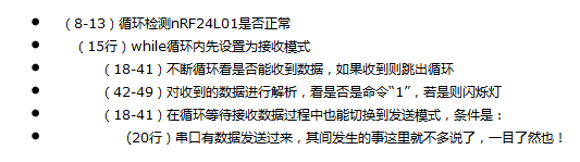
 1 void main()
 2 {
 3     LED = 1;                //初始灯6熄灭
 4     uart_flag = 0;            //串口标志初始为0
 5     nRF24L01_Init();        //初始化24L01
 6     UART_Init();            //初始化串口
 7
 8     while(nRF24L01_Check())                    //检查不到24l01则报警
 9     {
10         LED = 0;
11         delay_ms(200);
12         LED = 1;
13         delay_ms(200);
14     }
15     while(1)
16     {
17         nRF24L01_Set_RX_Mode();                            //接收模式
18         while(!nRF24L01_RxPacket(Rx_Buf))     //等待接收数据,返回1则接收到数据,在等待接收数据期间,可以随时变成发送模式
19         {
20             if(uart_flag == 1)                //当串口接受标志为1表示有数据过来
21             {
22                 ES = 0;                               //关串口中断
23
24                 nRF24L01_Set_TX_Mode();                         //发送模式
25                 Tx_Buf1[0] = a - '0';                    //将串口数据给发送缓冲区
26                 nRF24L01_TxPacket(Tx_Buf1);        //发送命令数据24L01
27                 UART_Send_Byte('O');            //向串口发送已经传送
28                 UART_Send_Byte('K');
29                 UART_Send_Byte(':');
30                 UART_Send_Byte(a);
31                 UART_Send_Byte('\n');
32                 LED = 0;
33                 delay_ms(300);
34                 LED = 1;
35                 delay_ms(300);                    //发送后LED1闪一下
36
37                 ES = 1;                            //允许串口中断
38                 uart_flag = 0;                      //中断标志位置0
39                 break;                            //退出最近的循环,从而变回接收模式,这句关键
40             }
41         }
42         if(Rx_Buf[0] == 1)                               //若接收到对应的数据则实现对应功能
43         {
44             Rx_Buf[0] = 0;                //清空数据
45             LED = 0;
46             delay_ms(300);
47             LED = 1;
48             delay_ms(300);                //接收到数据 后闪烁
49         }
50     }
51 }
小结&计划
至此,算是马马虎虎封装了一传感器、一个显示器、一个通信模块。是不是我们可以着手做一个组合型的更有意思的东西了?还太早!因为我们无论是串口还是2.4还是蓝牙,都仅仅实现通信,并没有采取必要措施保证通信的可靠与稳定,所以接下来一段时间我们将会在底层通信物理层上继续封装高层稳定的通信协议~敬请期待!
链接
希望这些资料对大家有帮助
大家顺手点个赞支持一下(⊙o⊙)哦
大晚上的,不容易丫!

http://pan.baidu.com/s/1jG2HotK
@beautifulzzzz
2015-10-9 持续更新中~
 浙公网安备 33010602011771号