OpAmp Voltage Follower/Regulator
LDO Regulator
High accuracy voltage regulator
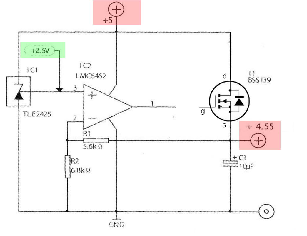
Vout = 2.5V * (1 + ( 5.6 / 6.8 ) ) = 4.55V
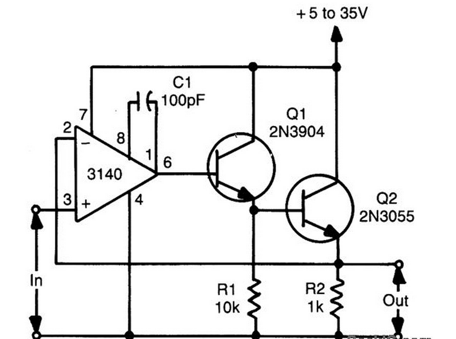
Recently the author had to adapt a standard circuit configuration (which often uses an npn bipolar)
so as to operate as a low-dropout (LDO) regulator.
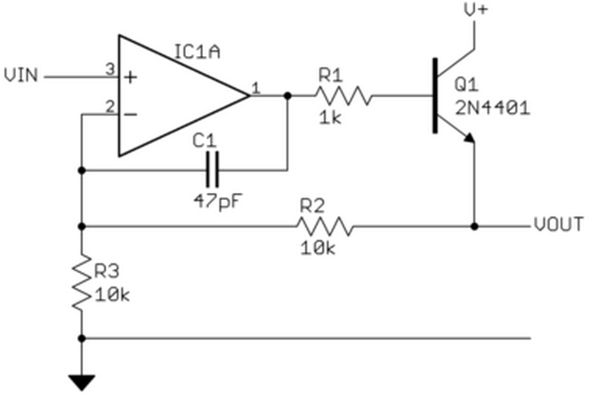
The circuit shown here uses that rarity, a depletion-mode MOSFET to implement the LDO function.
What to do when you have to derive an analogue supply voltage (close to +5 V) from an existing ‘digital’ 5-volt rail,
ensuring sufficient decoupling between the two?
One answer is to step up and then use a linear regulator to step back down.
However, if around 4.5 volts will suffice then an alternative is a home-made LDO regulator. [ 5.0 - 4.5 = 0.5 Vdrop ]
The circuit is usually a fairly standard shape typically a npn transistor (with base-current limiting resistor) is used.
Initially, it would appear that this design suffices after all, the text books say the saturation voltage is around 0.2 V.
Unfortunately, this is no longer true when the collector is tied directly to the positive supply.
An enhancement-mode NMOS MOSFET suffers similar disadvantages:
with the drain tied High you need greater than drain potential at the gate to achieve low RDS(on).
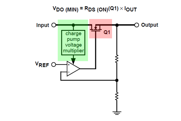
Enter that seldom-used beast the depletion-mode MOSFET!
Depletion-mode MOSFETS are ‘on’ even when V gs = 0,
and you have to back-bias the gate to achieve an increase in channel resistance.
In the circuit shown the BSS139, an NMOS depletion device, operates with the gate forward biased.
With a load of 10 mA, the measured FET resistance was 38 ohms. 10 * 38 = 380 mV = 0.38V
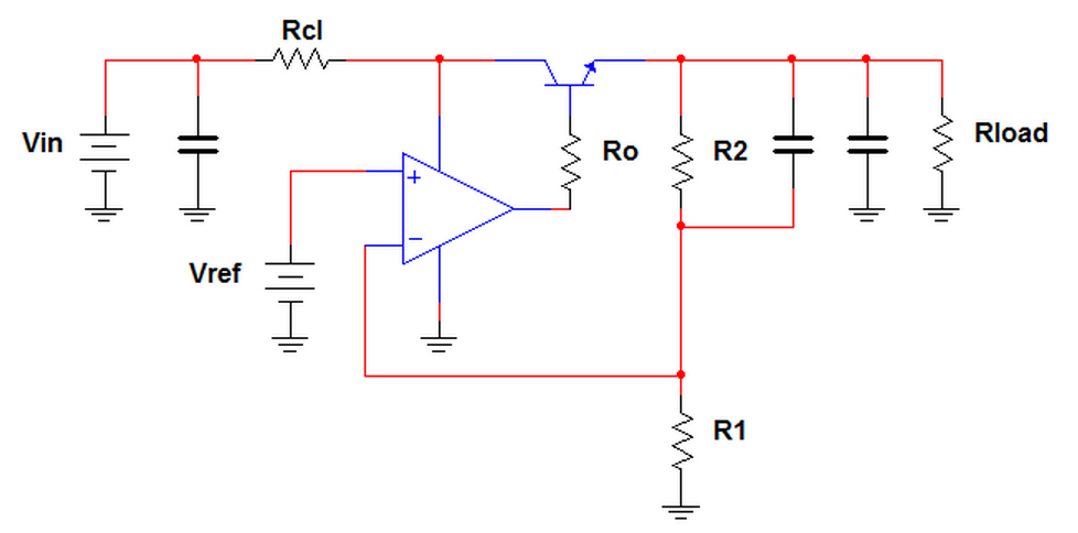
Voltage Controlled Voltage Source
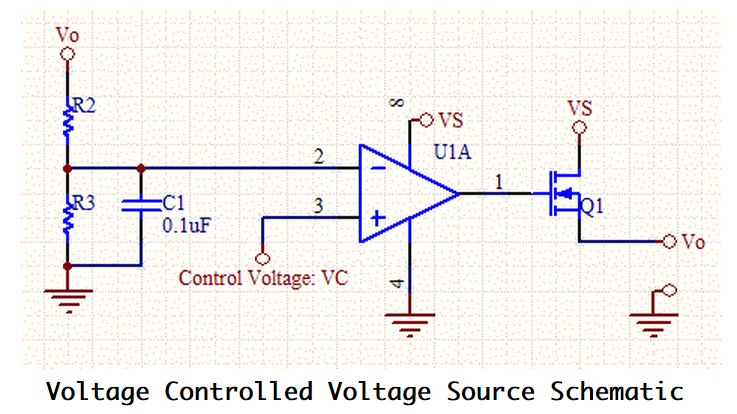
This circuit allows a smaller control voltage to linearly control a larger output voltage Vo.
The Resistors R2 and R3 scale the feedback to an appropriate range for the opamp.
R3/(R2+R3) = VCmax/Vo
Note: VS>Vomax+Vgs(th).
The disadvantage of the circuit above is that the supply of the op-amp is tied to the HV supply.
Most op-amps are limited to around 30V on the supply, so the circuit wont work for higher output voltages.
The circuit below avoids this this problem by inserting a n-channel mosfet,
which can be fully controlled within the range of the op-amps power supply.
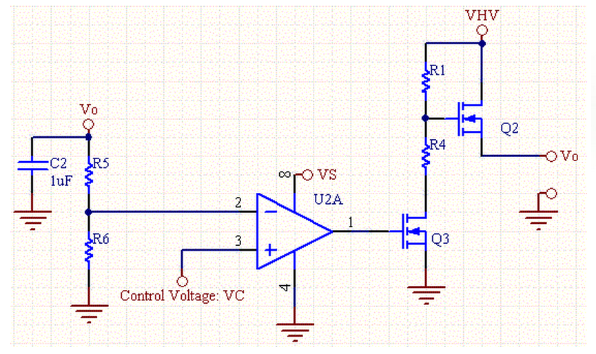
Voltage Controlled Voltage Source with N-Chan MOSFET Schematic
The output voltage is directly proportional to the control voltage.
R1 and R4 should be chosen such that Vgs(max) of Q2 is never exceeded.
Likewise Q2 should have an Idss greater than VHV.
Vgs(max)is typically around 20V for many MOSFETs. So the following should apply: VHV*R4/(R1+R4)< Vgs(max)
The feedback resistors are set according to this equation: R6/(R5+R6) = VCmax/Vo Vo= (R5+R6)/R6*VC
By using an emitter-follower or a Darlington pair,
a voltage-follower op amp configuration can source higher currents than the op amp otherwise could.
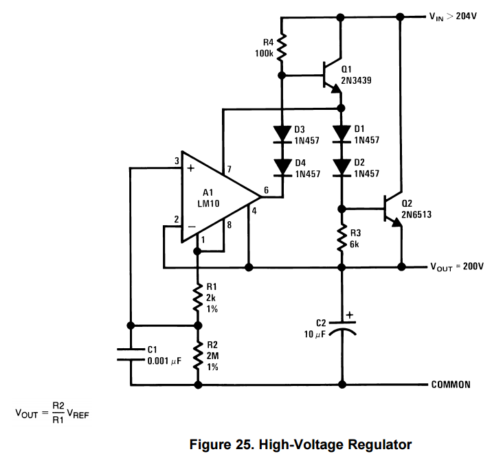
With high-voltage regulators, powering the IC through the drive resistor for the pass transistors can become quite inefficient.
This is avoided with the circuit in Figure 25.
The supply current for the IC is derived from Q1.
This allows R4 to be increased by an order of magnitude without affecting the dropout voltage.
Selection of the output transistors will depend on voltage requirements.
For output voltages above 200V, it may be more economical to cascade lower-voltage transistors.
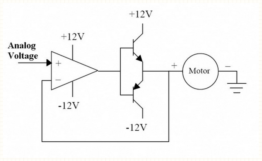
current buffer (voltage follower)
This is really simple - use an N channel FET and have it as a source follower.
You can even use a BJT.
The one below has gain due to the 3k3 feedback and the 1k to ground from -Vin.
If you don't want gain connect the output directly to -Vin and omit the 1k.
Quite simply the feedback on the op-amp tries to maintain the emitter at precisely the same voltage as Vin.
A unity gain buffer on the output of an op-amp is either an emitter follower or a source follower.
Simple as that - feedback from the emitter/source back to inverting input of the op-amp.
Additionally, because the source/emitter voltage "follows" the op-amps output signal,
the gate/base loading effects are minimal hence when using a MOSFET you don't need to worry about gate capacitance.
Think about this sensibly - Analog Devices or TI or MAXIM of LT - their marketing team are not going to wake up one morning
and say to their designers - why can't you design an op-amp that allows someone to add a gain stage on it and expect it to be stable.
If they did, the designers would say that they'd have to reduce the performance of the op-amp for it to be stable
- just how would that op-amp compete in the market against all the op-amps that take the sensible road and keep building what they are good at.
The output equals the input because the op-amp has to have both inverting and non-inverting inputs at the same voltage.
OK choose an op-amp that has low Vos and low Vos drift.
Choose an op-amp that has a very low noise figure if the sensor circuits you are feeding are used for very small measurements.
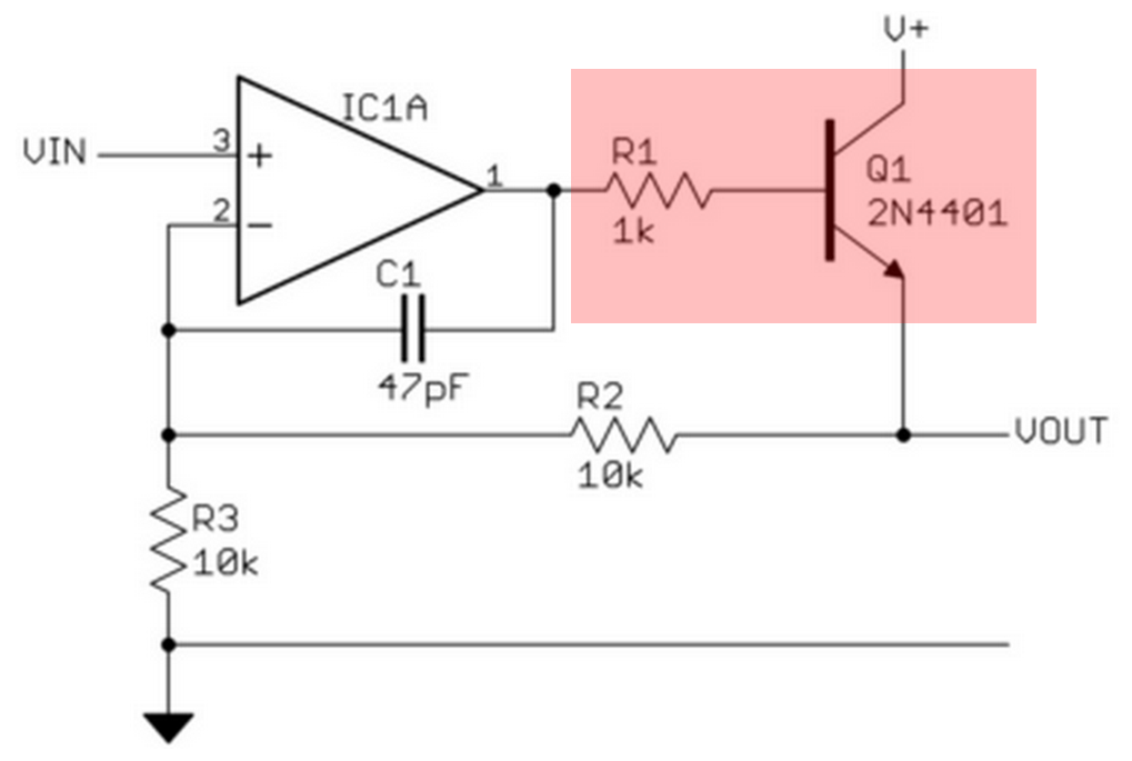
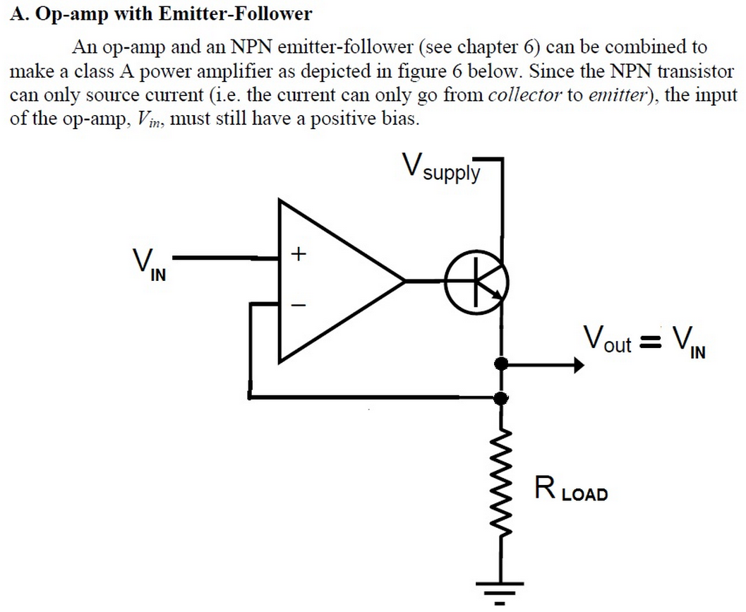
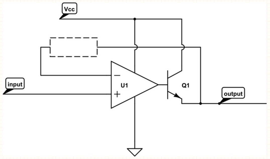
If your goal is simply to increase the current sourcing capability of an op-amp, the canonical way to do it is:
A transistor used in this configuration is known as an emitter follower.
The configuration is also known as "common collector", since the collector is shared between the input and the output of the transistor.
Your feedback elements go in the dotted box according to what you want the op-amp to do, just as if you hadn't added the transistors.
By incorporating Q1 in the feedback loop, the op-amp's gain will make significantly reduce any non-linearities in the transistor.
Further, if you already have an op-amp circuit that does what you want, except you need it to source more current,
adding the transistor this way won't significantly alter the function of your circuit.
If you also need to sink current:
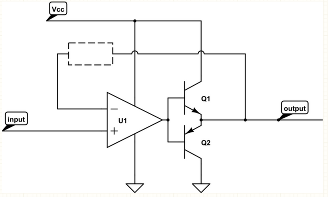
This configuration, where one transistor sources and the other sinks current, is known as push-pull.
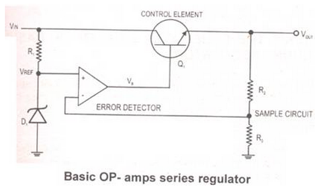
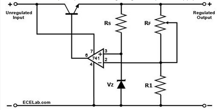
Op Amp Regulator with Series-Pass Transistor

What is the function of a voltage regulator circuit? It’s basically this -
maintain a precise voltage regardless of the current drawn by the load. Three basic components are needed to achieve good voltage regulation.
1. A precision reference (zener diode) to set the output voltage.
2. A muscle component (transistor) to deliver the required current.
3. An automatic controller (opamp) to adjust the transistor drive.
The “prime directive” of the op amp is to adjust the base drive of Q1 delivering the required load current
while keeping the output voltage at a fixed value.
OUTPUT VOLTAGE
Resistors RF1 and RF2 feed a fraction of the regulator output Vo to the op amp's negative input V-.
The op amp then adjusts the drive to Q1 such that V- is equal to the zener voltage Vz.
When this occurs, the output voltage is related to the zener voltage through the RF1, RF2 divider by
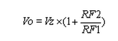
With the zener voltage at about 3V and RF2=10k, RF1=5K,
the output voltage should be 3 x (1+10/5) = 9V.
If you only need to source current and not sink it as well,
you could get by with a garden-variety op amp and a pass transistor.
Here's the basic topology:
Here is another circuit, similar to Phil's, except it uses an NPN transistor
with the output taken from the emitter instead of a PNP with output taken from the collector.
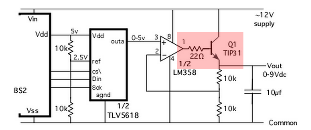
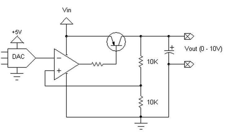
This circuit uses one of the two DAC outputs of the TLV5618 12 bit DAC.
The power supply has to at least 3 or 4 Volts above the desired output,
because of overhead of the LM358 op-amp plus the overhead of the transistor.
There are better choices for the output transistor and op-amp if you have constraints on the input power supply.
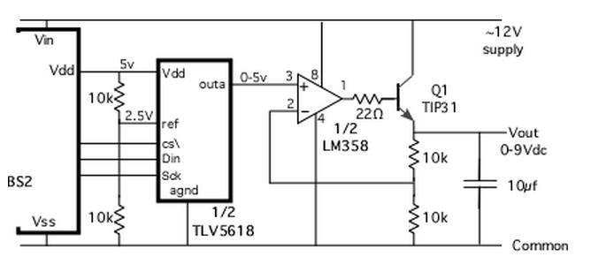
In terms of circuit configurations, in Phil's circuit with the PNP, the transistor common emitter gain is inside the feedback loop,
which makes it harder to stabilize and it will require a relatively large output capacitor.
The NPN follower gain is x1, which makes it easier to stabilize with a small capacitor.,
and base current contributes to the output current.
But the PNP circuit is the best if you need to operate very close to the power supply rail.
Another option, if you really don't need to get down to zero volts,
is to use a standard voltage regulator controlled by a digital potentiometer.
Those usually have a minimum voltage of something like 1.25 volts.
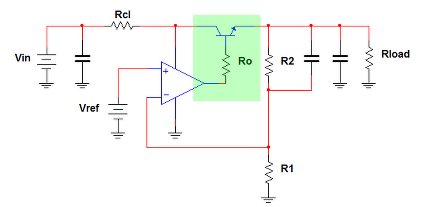
Voltage regulator with op amp(negative feedback) and MOSFET
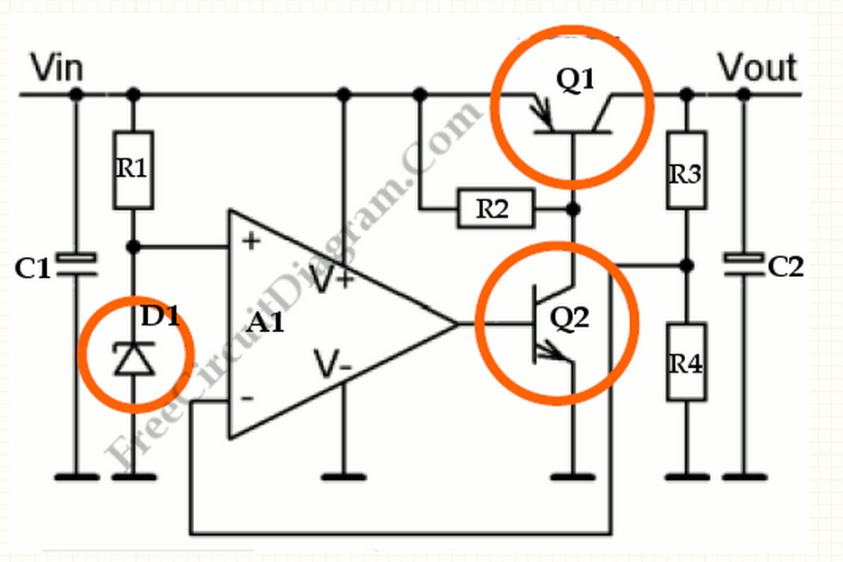
The schematic above is a very good voltage regulator, excepting the high power dissipation for Q1 (also I'd use an NPN instead of a PNP).
Can I replace Q1 and Q2 with a high current n-mosfet and expect the same behavior?
A mosfet has lower power dissipation than a bjt.
It's also not a very good voltage regulator unless Vin is already regulated :
the voltage across zener D1 is somewhat dependant on the current, which is (Vin-V(D1))/ R.
That dependence, or "slope resistance" of the Zener differs for different voltages of zener diode.
I'd also say it's not guaranteed to be a good regulator in general applications
because there is a good chance it will oscillate unless A1 is a very poor op-amp.
You can't say it's a good regulator without knowing what the component values are too.
Ditto Brian's comment about the zener and I'd add that if there was significant impedance in the line feeding it it'd be even worse!!
To make the new circuit work the same way as the existing one,
you'd need to replace Q1 with a p-channel MOSFET, not an n-channel one.
However, you would not save any power dissipation by doing this.
Because you wouldn't operate the MOSFET fully switched, you'd be operating it as a variable resistor.
You can see that there's no way to significantly improve the power dissipation of this circuit by the equation for device power:
P = I * V.
In this circuit, the current through Q1 is equal to the load current, so you can't change that.
And the voltage across Q1 (collector to emitter) is equal to Vin - Vout, and you can't change that.
So no matter what you replace Q1 with (however good a MOSFET you find), the power dissipation will still be
Iload * (Vin - Vout).
If you want to reduce the power dissipation from your regulator,
you need to look to a totally different type of circuit, like a buck switching regulator.
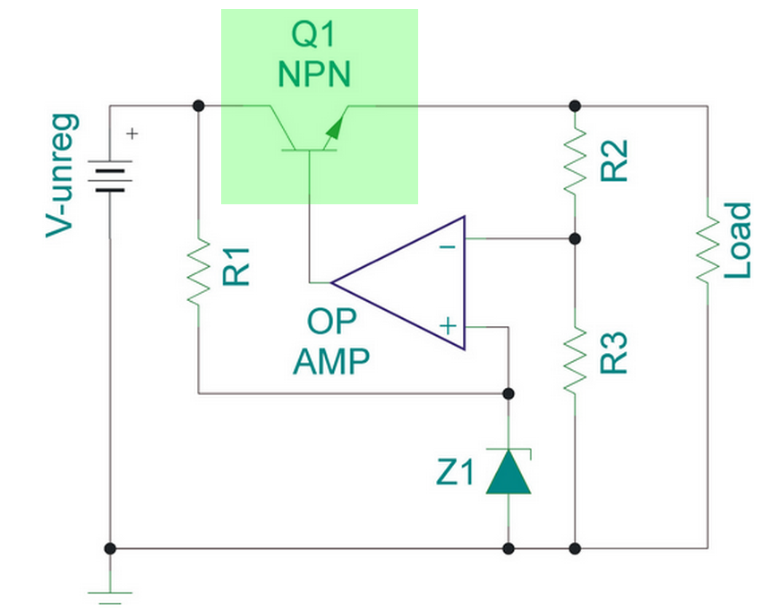
Here is another op-amp based voltage regulator/power supply:
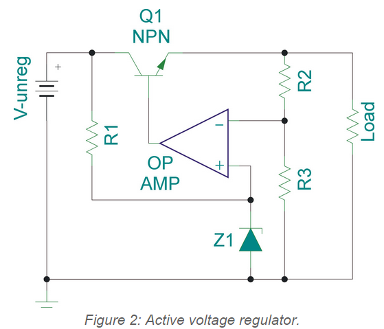
The Zener diode (Z1) provides a stable reference at the positive input of the op amp.
The op amp adjusts its output until the sample voltage at the negative input formed by the R2-R3 voltage divider equals the Zener voltage.
Output voltage control is then maintained over a wide range of load current and input voltage.
Unfortunately, this circuit is not very efficient.
Efficiency can be significantly improved with switching regulators.
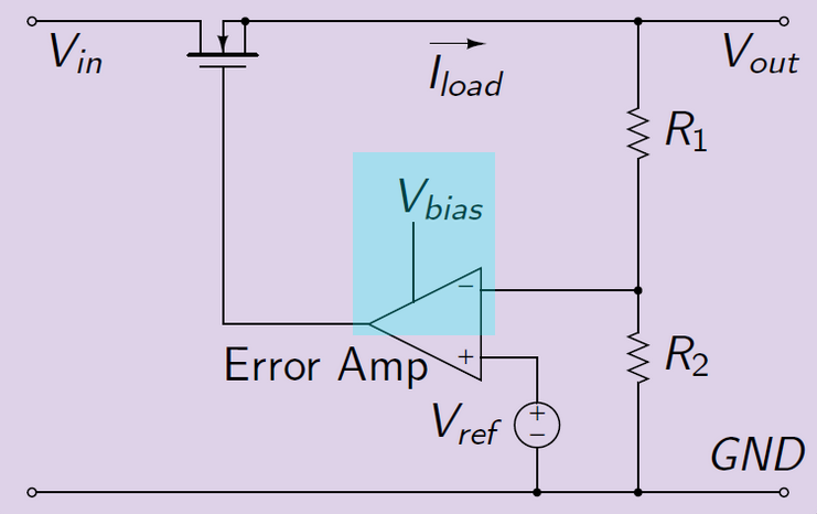
Fixed output voltage feedback networks
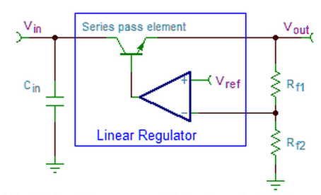
A linear regulator includes an error amplifier that compares the voltage applied to its feedback pin to an internal reference.
The regulator contains a controller with a feedback voltage amplifier that compares an external voltage,
derived from the regulator's output voltage through a resistive divider network, to a fixed internal voltage reference.
The output of the error amplifier drives a series pass element, or power stage, which delivers current to the output.
By setting the external resistors, Rf1 and Rf2, you can set the regulator's output voltage
to any voltage greater or equal to the internal reference.
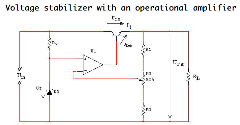
In this case, the operational amplifier opens the transistor more if the voltage at its inverting input drops significantly
below the output of the voltage reference at the non-inverting input.
Using the voltage divider (R1, R2 and R3) allows choice of the arbitrary output voltage between Uz and Uin.
Are opamps as a voltage regulator effcient?
If I setup an opamp in a non-inverting configuration as follows:
Vrail+ is 7.5V, Vrail- is GND (0 V)
Vin is 2.5V, Vout = 3.3V (in other words, the gain, aka, 1+R2/R1 is 1.32 [V/V])
Iout = 100mA (connected to some load)
What are the source of my losses? How efficient are these types of configurations?
Do I only take the quiescent current as the only loss?
Opamps can't usually supply 100 mA.
But, they can still be used to control a power voltage if you add some current gain to their output.
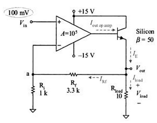
If you really want a opamp to control a power voltage that can supply 100s of mA, here is a simple way:
The opamp still does the controlling and still provides voltage gain from Vin to Vout.
However, Q1 provides most of the Vout current.
R2 and R3 are the voltage feedback and the overall gain is the reciprocal of their attenuation ratio.
In this example R2 and R3 are equal, so the voltage gain from Vin to Vout is 2.
You might think all you need is the transistor and R2 and R3, but that could be unstable.
To make the opamp stable, you put a small cap directly between its output and inverting input.
But, you also need to let the opamp output not be loaded directly with the end load, especially if that load is capacitive.
R1 decouples the opamp output from the load such that the opamp should be able to reach whatever output voltage it wants to.
Without that, the stability feedback provided by C1 won't work right and the thing can oscillate anyway.
The best value of C1 is hard to predict, so start with something vaguely plausible, like I show, and then experiment.
Making it lower will invite instability and result in oscillations.
Making it higher will dampen the response to transient loads.
Test by connecting the worst case non-resistive load you expect,
find the value of C1 just where it starts to be unstable, and then double it in the real circuit.
However, stepping back a couple of layers in this case, you don't need a opamp voltage regulator
since the voltage you want is both a common value and known up front.
There are plenty of 3-terminal linear regulators specifically designed for this task that can source 100 mA.
If it's OK to waste the extra power as heat in the linear regulator, then this is clearly the way to go in your case.
In this case you're dropping 7.5V - 3.3V = 4.2V, which times 100 mA is 420 mW.
A linear regulator in a TO-220 or similar case will get warm, but won't require a heat sink.
If efficiency or getting rid of heat is a issue, then use a buck regulator to make the 3.3 V supply from the existing 7.5 V supply.
You won't be able to supply 100mA from all standard op-amps -
maybe 20mA for most and up to 50mA for more specialist devices.
There are such things as power op-amps that can deliver amps but these are specialist devices.
Regarding efficiency - the power delivered to the load might be 3.3V x 20mA = 66mW
and the power into the opamp will be 7.5V x (20mA + ~5mA for the op-amp) = 187.5mW.
The quiescent current of the device may be 3mA rising to 5mA to produce the output current.
There's a bit of hand-waving but even if you ignored any current taken by the op-amp
you still have 7.5V powering it and 20mA being delivered to the load = 150mW.
If you ran the op-amp from a 5V supply it would be better but remember it is a linear device
that isn't like a switch mode power supply - if your output is 20mA this 20mA gets taken from the op-amps power rails.
This circuit gives the output voltage as is set for (maximum output is limited by the rails)
but it will not be well regulated anymore at higher load.
This also depends on the strength of the op amp of interest.
There are lots of high current capability (Amperes) op amps available now out there.
This circuit isn't a voltage regulator by any chance.
It'll oscillate with high capacitive load, and can't sustain line or load transients.
Voltage Regulator Calculator
This calculator was created to give the designer the optimum values for voltage regulator set resistors,
given a value for the reference voltage. See the description below the calculator for more
Can I use an op-amp in voltage follower configuration
as variable voltage power supply?
I see that this works in theory, but I my gut feeling says there is a drawback or caveat of which I'm not aware.
Basically what I want to achieve is described best by the circuit diagram below.
I have a power supply (2A @ 12VDC) that I want to use to make a variable voltage power supply.
In the voltage follower configuration, whatever is on the non-inverting terminal on the op-amp is present on the output terminal.
The extra current at the output terminal needed to keep the voltage up is provided by the op-amp's supply.
Since I'm using a linear pot as a voltage divider to set the input voltage to the op-amp,
will this work as an effective variable power supply from 0V to almost 12V?
If not, why can this configuration not be used this way?
The problem is that the output current from most op amps is weak at best.
If you use the op amp to control a P-type high-side transistor instead then you'll have yourself a LDO regulator.

It can be used but for most op-amps the maximum current
you would be able to drive from the output will be limited to less than 50mA.
Op-amps are not miracle workers!
On the other hand you can attach an NPN and PNP transistor in a push-pull configuration and get more current: