
Programmed Adjustable Power
Programmed Adjustable Power
I just explored an easy scheme to design a high precision programmed adjustable power.
In this scheme, there is no needs to make a complex PWM circult,
just a liner or switcher adjustable voltage regulator and a resister network, a DAC, and a MCU.
Resister network change DAC output voltage into feedback voltage
and let adjustable voltage regulator regulate output voltage itself.
Outputting an fixed voltage by using resister to control regulator may be easy,
but there is a little challenge to output adjustable voltage.
My mates used to use digital potentiometer to adjust output voltage, but digital potentiometer is too instable.
Lucky, DAC with a resister network works better, and they can provide high precision output witch depends the resolution of DAC.
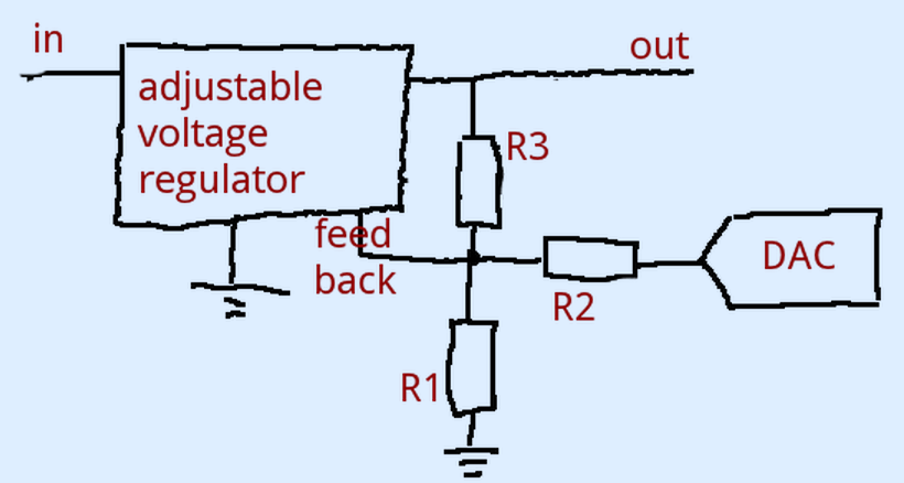
In this figure, voltage of the node feedback is fixed by the Vref (OR Vsense) of regulator.
LM2576 is 1.23V, TPS5432 is 0.808V.
When there is voltage difference between Vout of DAC and Vref of regulator, the difference sets up an current in R2.
Then the current through R1 to the ground.
This adjustable current could change the resistance because voltage between Vref and GND is fixed
and no current will go into Vref pin duo to the virtual short and virtual open of the error amplifier inside of the regulator chip.
Now it's time to value R3, R2, R1.
Make sure that the output range of this regulator (Vout) and DAC (Vdac) , and Vref by checking the datasheet of part.
Then, list two equation.
(Vdac.max-Vref)/R2+(Vout.min-Vref)/R3=Vref/R1
(Vdac.min-Vref)/R2+(Vout.max-Vref)/R3=Vref/R1
Three unknown resistance, but two equation, we must assume the value of R3. 10K is very common.
Then check the Idac.max to make sure that DAC will not overloaded.
[Update 2014/Tue/22] PS:
Three terminal regulator, such as LM317 is not available to this equation because the 1.25V is between Ref pin and out pin.
We use TI's TLC5615, 10-BIT DIGITAL-TO-ANALOG CONVERTERS as our DAC.
This chip has 3-Wire Serial Interface, so we can use Arduino to control it.
Arduino is an open-source physical computing platform based on the AVR MCU.
Now give the Arduino program.
//Arduino project http://arduino.cc
//by Mini Dragon at http://minidr.com/archives/687
//This program is licensed under a Creative Commons Attribution-ShareAlike 3.0 License.
#define CS 2 //chip enable
#define CLOCK 3
#define DATA  4

#define HALF_CLOCK_PERIOD 2 //2 uS of clock period
float j=0;
void setup()
{
    pinMode(DATA, OUTPUT);
    pinMode(CLOCK,OUTPUT);
    pinMode(CS,OUTPUT);
    digitalWrite(CS,HIGH);
    digitalWrite(DATA,LOW);
    digitalWrite(CLOCK,LOW);
}

void writeValue(uint16_t value)
{
    digitalWrite(CS,LOW);//start of 12 bit data sequence
    digitalWrite(CLOCK,LOW);
    data = data << 2; //Add 2 0 at the end of the data. A 10-bit data word should add 2 0 at the LSB bit (sub-LSB) since the DAC input latch is 12 bits wide.(SEE TLC5615C DATASHEET)
    for(int i=11; i>=0; i--)//send the 12 bit sample data
    {
        digitalWrite(DATA, (value & (1 << i) ) >> i );//DATA ready
        delayMicroseconds(HALF_CLOCK_PERIOD);
        digitalWrite(CLOCK,HIGH);//DAC get DATA at positive edge
        delayMicroseconds(HALF_CLOCK_PERIOD);
        digitalWrite(CLOCK,LOW);
    }
    digitalWrite(CS,HIGH);//end 12 bit data sequence
}

void loop()
{
    j=567; //in here, 567 is a example. DAC OUT=j*Vref/1024
    writeValue(floor(j));
}
Each DAC output voltage maps a main Vout.
Long day for me to update my blog. I even don't know my blog was blocked by our Great Fire Wall.
Yesterday I passed my first time of GRE test.
That's a f**k test.
But during the day of preparing the GRE, I got a chance to attend our University's electronic design contest.
In the contest, I fixed some problems of my power and add some now function into it.
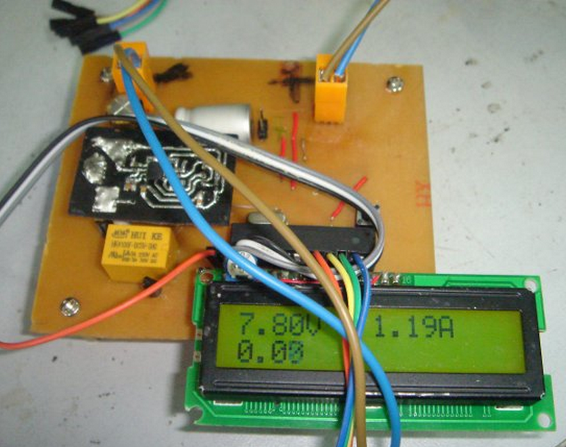
This is the top layer of the power.
You can see a black PCB which plug into the main board.
That's a current detection module.
I using TI's INA200A to detecting the current of power's output.
Then using Arduino's ADC to check out the current if the current exceeds the threshold value.
This threshold value could change during the runtime.
If the power is overloaded, the relay (yellow thing) will cut off the output to protect the buck chip until manual reset the system.
The 1602 LCD could display the output voltage, output current and cut off thrshold current value.
Using Arduino to control the LCD is very simple like using printf() function in C language.

This the bottom layer of the power. I using the surface mount package part to keep the system small.
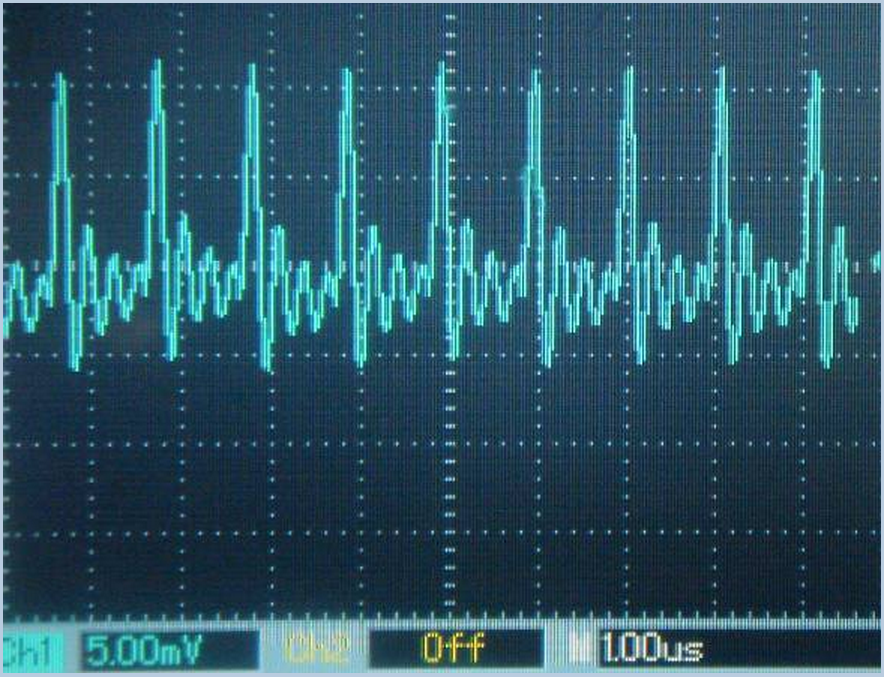
This is the out put waveforms.
About 15mV ripple voltage in 1A load, 10V output.
Fantastic result by using Nichicon HD aluminium electrolytic capacitor.
That's all of the
This project is open-sourced, under the licence of BY-NC-SA.
If you want the SCH, PCB file and Arduino file, leave the comment and I will mail you ASAP.
Thanks to Texas Instruments for offering me so many kind of chips free.
dfd

