ARM JTAG 信号 RTCK 应该如何处理?
用户在调试内嵌可综合内核的 CPU 如 ARM7TDMI-S 时,需要通过打开仿真器的自适应时钟功能。
此时,ARM仿真器根据 RTCK 时钟信号的频率,产生可用于 CPU 内核当前时钟主频的最快的 TCK 时钟。
即 ARM 内核的时钟主频变化,引起 RTCK 变化, 仿真器根据 RTCK 的变化,产生合适的最快的 TCK 时钟。
如果没有有效的 RTCK 信号,用户不能使用自适应时钟功能。这种情况下,用户可以设置 TCK 为比较低的频率。
当用户确认 CPU 运行在比较高的频率的情况下,可以手工调整 TCK 到比较高的频率。
如果用户不使用自适应时钟功能时, JTAG 插座上的 RTCK 可以直接拉低。
S3C2440中JTAG 20管脚调试接口中RTCK管脚功能
数据手册中表明:RTCK-返回的测试时钟输出。
JTAG 端口的额外信号。当处理器频率变化时帮助调试器保持同步。
带内部上拉的双向口。当RESET 为低时,RTCK 上的低电平会使
P1.26~P1.31 在复位后作为调试端口。但是RTCK管脚可以不接。
RTCK from target to adapter, Some chips are entirely controlled by a single clock,
where TDO changes are possibly asynchronous to TCK.
The re-synchronized RTCK can be used by the JTAG adapter to deal with asynchronous TDO signals.
The adapter will not change TCK until it gets back the RTCK edge from a previous TCK change.
This results in a second advantage, because the adapter can dynamically adapt the JTAG clock rate to the target's ability.
If, for example, the target is switched to sleep mode and running on a reduced main clock,
it may not be able to handle full speed JTAG clocking.
The CoreSight DAP (SWJ-DP or JTAG-DP) has no need for an RTCK.
RTCK is not a standard IEEE 1149 JTAG signal.
It was created to allow the use of synchronized TAP controllers in ARM9 and ARM11 class of cores,
where the JTAG inputs (TMS and TDI) have to cross an asynchronous boundary into the processor clock domain.
RTCK has the effect of controlling the TCK from the emulator box (RVI, Multi-ICE, etc)
to ensure correct JTAG-like behaviour across that clock domain boundary.
The CoreSight implementation of the DAP uses a fully asynchronous TAP controller
which does not require any local synchronization (hence no need for RTCK).
It manages the asynchronous relationship between JTAG (TCK) and the DAP bus (DAPCLK/PCLKDBG) internally to the JTAG-DP or SWJ-DP.
TCK can be run at any frequency up to the maximum operating frequency of
your ICE unit + interconnect (wires, connectors, board traces) + TAP logic in the TCK domain.
TCK frequency is not dependent upon the core clock frequency in a CoreSight system.
Adaptive Clocking
Description
The ARM Ltd. ARM 9 and ARM 11 implementation of JTAG is not compliant to the IEEE1149.1 specification.
This is because the user must make sure the next TCK edge to the device is not provided before the device generates a RTCK edge.
This function of the Emulator is called Adaptive Clocking.
Most ARM emulators support adaptive clocking which:
- Ensures that TCK is running at the highest possible frequency no matter what the ARM clock is.
- Automatically scales TCK as the ARM clock scales.
- Ensures that chip is not presented with another TCK edge until an edge is detected on RTCK.
- TCK clock generation is essentially a NOT gate on RTCK.
- TCK is not a free-running clock.
- TCK is nearly completely out of phase with RTCK.
Summary
- Lack of Adaptive Clocking Makes debuggers (ex: CCS) look unstable.
- The key problem is a violation in the specification.
Attempts to fix in the chip have been attempted, but have not been consistently successful.
- Use of Adaptive clocking will result in:
- Higher performance (downloads, etc.) than without Adaptive clocking.
- Greater Stability
Solutions
- Adaptive clocking emulator
- This solution is the most reliable and best performing.
- XDS560 Revision D and later products have adaptive clocking capability. XDS560 Emulators
- 3rd party emulators from vendors such as Lauterbach, Green Hills, etc. may have adaptive clocking.
Please contact your vendor to check support for this capability.
- Reduced TCK speed
- Most processors made after 2007 have some integrated support for adaptive clocking.
Slowing TCK to the legacy 10.368 MHz speed is generally sufficient to use an older XDS510 emulator with these devices. - If the 10.368 MHz speed still does not allow for a stable connection you can further slow it down, perhaps as low as 1 MHz, for better stability.
- Most processors made after 2007 have some integrated support for adaptive clocking.
- Adaptive clocking Adapter
- This solution is only recommended for older devices that did not integrate any adaptive clocking support into the processor
(e.g. OMAP5910/12, DM6446, etc.). It is not recommended to use this adapter with newer devices that already have integrated adaptive clocking support.
For example, using one of these adapters with DM6467 will actually make the connection less stable. - Adaptive Clocking Adapters are available from TI:
Adaptive Clocking Adapters Note that you do not need an adaptive clocking adapter
if your emulator supports adaptive clocking (ex: XDS560 Rev D).
- This solution is only recommended for older devices that did not integrate any adaptive clocking support into the processor
- For multi-device Scan Chains, see below.
- For more details and configurations that include both devices that require adaptive clocking
and devices that don't require adaptive clocking on a single scan chain see XDS Target Connection Guide.
Multi-Device Scan Chain Connections with Devices that require Adaptive Clocking
- For cards which have multiple devices (ex: multiple ARM9 devices) that require adaptive clocking on a single scan chain, attention must be paid to ensure that the connection is stable and able to operate at a reasonable speed.
- As these devices require a RTCK signal, there are two connection methods which can be used. They differ mainly in performance and complexity.
Series Topology Connection
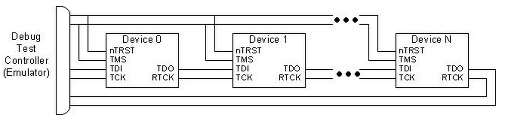
- Connecting devices with RTCK in a serial cascade fashion means the RTCK
from one device is synchronized with the TCK of the next device in the cascade,
and so on until the last RTCK is returned to the emulator.
- Series Topology can only be used when:
- a slow enough TCK freq to guarantee RTCK occurs before the next TCK edge, or
- a debugger which supports adaptive clocking (see Solutions above) is used
Parallel Topology Connection
- In order to operate in parallel, external logic must be used to co-ordinate the TCK and RTCK between the devices. *This is shown below
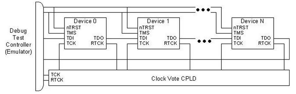
- This external logic must be designed to allow multiple devices with RTCK to be operated in parallel, rather than a serial fashion.
This method of operation provides higher performance than the series topology connection.
In order to operate in parallel, logic provides a TCK edge to each device simultaneously.
It then waits until every device has responded with an RTCK signal of the same polarity.
Once this has occurred, the opposite edge of TCK can be applied to the devices.
This repeats indefinitely. - Click here for Board level Clocking Voting Logic. Note that this Boad level clocking voting logic is offered as-is, without support.
What about ARM Cortex M3, R4, or A8 devices? Do these have RTCK?
- A: The ARM Cortex M4, R4, or A8 cores do not have RTCK, so are not affected.
However, some devices which feature these cores may also have an ARM9 which does require RTCK.
In those cases, if the ARM9/11 core is debugged, then RTCK must be taken into account.
For example, if you have 2 devices, each with a Cortex A8/ARM9, and you do not plan to debug the ARM9,
you could hook the emulator TCK to TCK input of both devices and pick the RTCK from either one to emulator RTCK.
ERROR: The RTCK Signal does not respond.
Can happen due to numerous of reasons:
- RTCK not connected
- RTCK signal doesn't exist for current target device
- Target device is wrongly connected
- Target device is not powered on
- Target device hardware is malfuncitoning
- If target device pinout contains RTCK signal pin, connect it
- If target device doesn't contain RTCK signal pin, use fixed TCK value
- Recheck connection according to provided JTAG target device pinout
- Make sure that target device has sufficient power and
that power on sequence is executed (Connect USB cable, charger, or simply hold power on key) - Check target device hardware
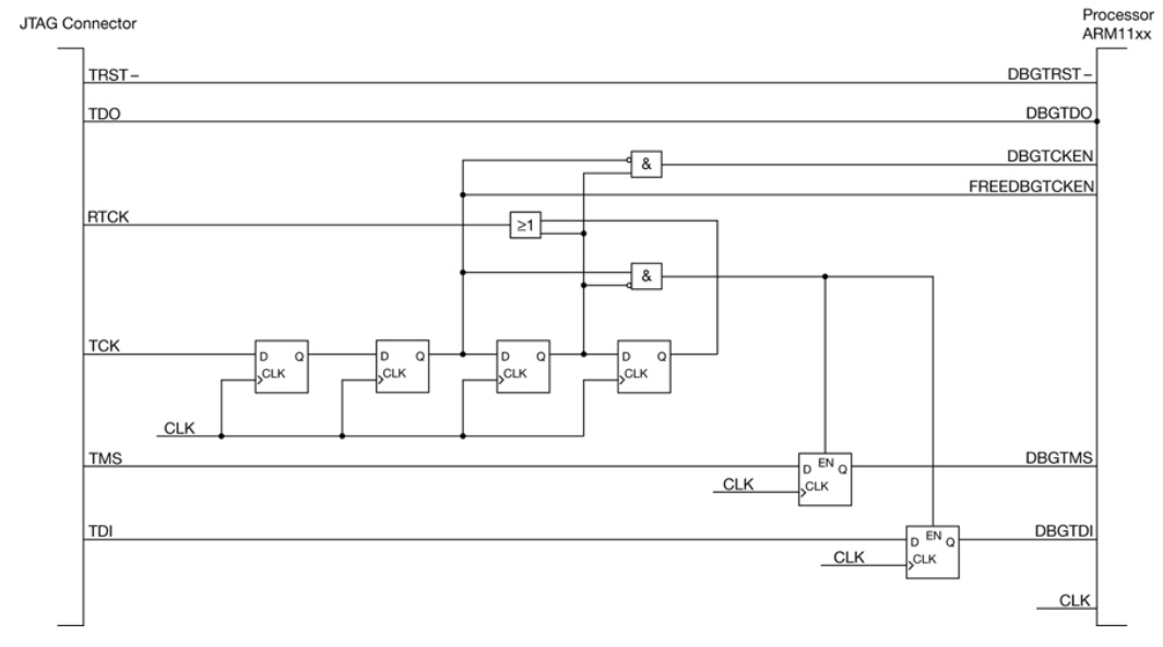
How does the JTAG synchronisation logic work?
How does adaptive clocking work?
Synthesizable cores need to implement a JTAG synchronisation logic block,
which samples TDI, TMS and TCK from the JTAG emulator with the core clock.
The synchronisation logic generates a signal called RTCK,
which is a synchronised (delayed) version of TCK.
The JTAG synchronisation logic is explained in the cores' technical reference manuals.
Below is a diagram taken from the ARM9E-S TRM.
If you configure the JTAG emulator (Multi-ICE or RealView ICE) in adaptive clocking mode, it uses the information in RTCK to generate TCK.
The JTAG tool waits to detect a falling edge in RTCK before generating the next rising edge in TCK :: TMS and TDI has clocked to DBGTMS and DBGTDI.
and waits for the rising edge of RTCK to generate the next falling edge in TCK :: DBGTDO and TDO is valid to be sampled by JTAG Tool.
There is a delay between the detection of an edge in RTCK and the generation of the next edge in TCK,
due to the time needed to sample RTCK with an internal clock.
This delay is different depending on the JTAG tool used.
- With Multi-ICE you can select a TCK frequency in either adaptive or non-adaptive mode. The delay is one half of the TCK period selected plus about 50ns
- With RealView ICE, if you select adaptive clocking, you cannot select a TCK frequency.
RTCK is sampled by default with a 50MHz internal clock, T = 20 ns
so TCK changes approximately 60ns after RTCK. 3T = 60 ns
This can be a problem when connecting to very slow targets such as hardware emulators.
The result of this is that the TCK frequency in adaptive clocking is not the highest possible, but it is close to it.
If you need to work at the maximum possible JTAG frequency you should disable adaptive clocking and set the JTAG speed manually.
The three sampling flip-flops set the theoretical maximum TCK frequency, which is one sixth of the core clock frequency (one eighth in ARM11).
The figure below shows the timing of the signals inside the three-stage JTAG synchronisation logic.
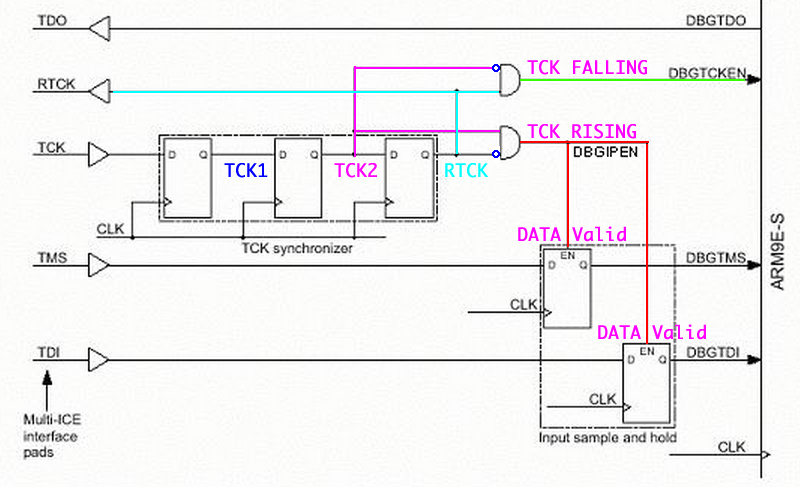

In position 1 the synchronisation logic registers TDI and TMS, so the falling edge of TCK (which changes TDI and TMS) must happen after position 1.
This imposes a minimum length of 3 CLK periods on the TCK high period.
In position 2 DBGTDO is generated by the core.
In position 3 TDO is sampled by the JTAG tool at the following rising edge of TCK (position 3).
This imposes a minimum length of 3 CLK periods on the TCK low period.
In order to avoid a racing condition in the sampling of TDI, TMS and TDO,
the real maximum TCK frequency will be lower than this and will depend on the core clock frequency,
the delays on the JTAG signals and the setup time of the JTAG emulator and the ASIC.
In adaptive clocking mode, the JTAG emulator ensures that there is some time
between the falling edge of RTCK and the rising edge of TCK and vice-versa.
This way the sampling of the JTAG signals is always correct.
Adding Adaptive Clocking Support to TI JTAG Emulators
What is Adaptive Clocking?
Adaptive clocking is a feature of synthesizable cores, introduced by ARM® Ltd. and adopted by TI in their OMAP platform,
wherein the input test clock (TCK) is delayed (synchronized) before producing the resulting output clock (RTCK).
During this synchronization period the target core samples Test Data In (TDI), Test Mode Select (TMS), and TCK with the core clock.
Emulators can adapt to the RTCK output of these adaptive clocking cores using a simple scheme.
This scheme requires the emulator to generate the next TCK edge only after receiving an “acknowledge” signal from the target,
indicating that it has received and processed the previous edge.
The target will “acknowledge” these TCK edges by repeating them (after some delay) on its RTCK output.
This protocol creates a natural, targetcontrolled “throttle” for the TCK rate.
A positive side-effect to this mechanism is that any delays introduced by the JTAG cable are automatically taken into consideration.
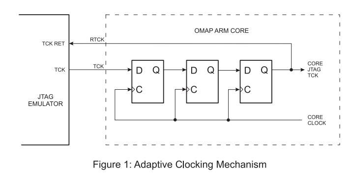
Internally, the adaptive clocking mechanism is implemented as a multi-stage synchronizer consisting of several D-Triggers
(Figure 1) synchronizing the TCK to the core clock of the target
(as well as transferring all other JTAG signals to the core clock domain).
The number of synchronizers, Ns, is device dependent, but has shown to be a value of 3 or 4 in OMAP cores at this time.
RTCK is the output from the last D-trigger and is typically connected to the TCK_RET pin of the JTAG connector.
The theoretical maximum TCK rate can be easily calculated as the frequency of the core clock divided by 2 times Ns (Equation 1).

Handling adaptive clocking is not obligatory, so emulators that do not support it should still operate.
They will, in general, just disregard the information on the RTCK pin.
The drawback of not using adaptive clocking will be the inability of the emulator to work at the optimum TCK rate.
If the emulator supports a variable TCK, the user will have to manually set the maximum
and sustainable TCK frequency through experimentation.
And if the device’s core has a variable clock rate, this RTCK can change during operation.
Another disadvantage for fixed TCK emulators is that they will have trouble synchronizing the data with the adaptive clocking cores.
For example, if the emulator has a 12 MHz TCK and the OMAP core is 24MHz, you’ll likely have data corruption.
Utilizing this feature adds convenience, stability, and increased performance, and is therefore strongly desired.
The Inverter Approach
The simplest solution is to have the emulator invert each RTCK edge to produce the next TCK edge (Figure 2).
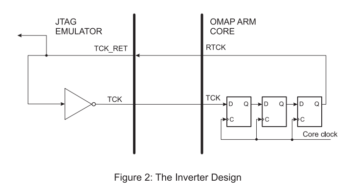
The main advantage of this approach is its ability to reach a TCK rate very close to the theoretical maximum.
The downside, however, is that the design is fully dependant on the target return clock and
cannot function with non-adaptive clocking targets.
This is because such targets usually have TCK_RET shorted to TCK on their JTAG connector,
forcing the inverter to produce an unusable TCK (“infinite TCK problem”).
The Trigger-Inverter Approach
A solution to the “infinite TCK problem” is to have the emulator
send the target an inverted version of RTCK as done in the inverter approach,
but only after sampling it with its own clock, referred to here as ETCK (Figure 3).
This method will make the emulator function with non-adaptive clocking targets,
but the maximum output TCK will be determined by ETCK.
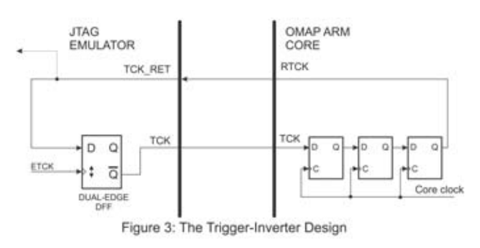
In this approach, the sampling of RTCK is best performed by a dual-edge D-Flip Flop (DFF)
to avoid halving the frequency of the resulting TCK, which would confuse those emulators that measure it.
Due to the added delay imposed by the DFF, the maximum TCK rate will be somewhat lower,
but will still be compatible with non-adaptive clocking targets, which is its major advantage.
The asynchronous relationship between ETCK and the target core clock introduces an inevitable jitter on the produced TCK.
This jitter (with a maximum value of 0.5TETCK) is harmless, and has the added benefit of introducing spread-spectrum modulation to TCK,
lowering EMI levels and improving EMC.
JTAG Emulator Implementation
We implemented both designs using Blackhawk™ JTAG emulators (models USB510 and USB560)
and tested them on a TI OMAP5912 processor with an ARM926EJS core running at 192, 96, 48 and 12 MHz as the adaptive clocking target.
The emulators had their TCK-related logic (contained in a 7-ns Xilinx® Coolrunner™ or Coolrunner II CPLD)
enhanced to accommodate the adaptive TCK support.
These units have total delay, tD = 15 ns (logic delay of 13 ns and line delay of 2 ns).
The maximum TCK for the OMAP5912 running at 192 MHz should have been fCORE/6, or 32 MHz,
but on accounting for the logic and line delays, we recalculated the actual maximum fTCK of OMAP5912 to be 19.2 MHz.
The Inverter Approach produced a jitter-free TCK at 12 MHz.
The Trigger-Inverter Approach also produced a 12-MHz TCK along with the expected jitter.
However, this design functioned correctly with non-adaptive clocking targets,
achieving similar maximum TCK frequencies as non-adaptive clocking emulators.
Adapter Board Implementation
We also implemented the trigger-inverter approach in a commercially available add-on adapter board (Blackhawk Adaptive TCK)
that enables adaptive clocking for any TI JTAG emulator lacking this capability (Figure 4).
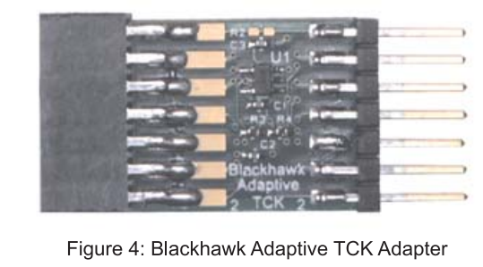


The adapter board is simply inserted between the standard 14-pin connection of the emulator
and target board and its operation is completely transparent to the emulator.
Figure 5 shows the fundamental logic of the adapter.
Since fast low-voltage CMOS (LVC) logic was used for this implementation,
the emulator reaches TCK frequency very close to the OMAP5912’s theoretical maximum of 19.2 MHz.
The characteristic jitter was also present.
The adapter board also functions correctly with non-Adaptive TCK targets at frequencies as high as 64 MHz.
As seen in Figure 5, the add-on adapter board also addresses a test reset (TRST) issue found
with XDS510™-class emulators built around the SN74ACT8990 Test Bus Controller (TBC) and certain OMAP targets.
This includes the TI XDS510 ISA card emulator.
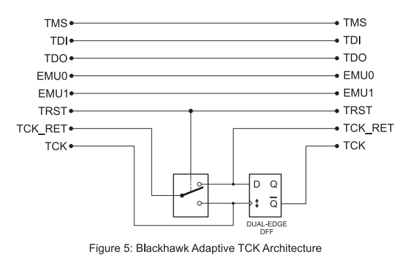
The issue appears in emulators that are dependent on the TBC device and use one of its pins to handle the TRST signal.
The problem occurs when some OMAP targets (e.g. OMAP DM320) stop their RTCK signal the moment TRST is asserted.
Since the TBC is clocked by RTCK, it will halt, keeping TRST asserted indefinitely and producing a deadlock.
The adapter board solves this condition by connecting the emulator’s TCK to TCK_RET during assertion of TRST.
This feature of the adapter board does not affect emulators that do not use a TBC pin to handle the TRST signal, such as the XDS560™.
Timing Analysis
Figure 6 shows TCK (upper waveform) and RTCK (lower waveform)
on an adaptive clocking target being debugged by an emulator that does not support adaptive clocking.
As the diagram shows, the emulator-supplied TCK is not adapted to the target RTCK speed requirements, forcing the latter to miss some of its edges.
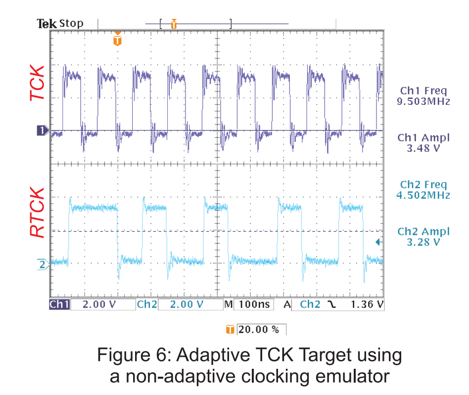
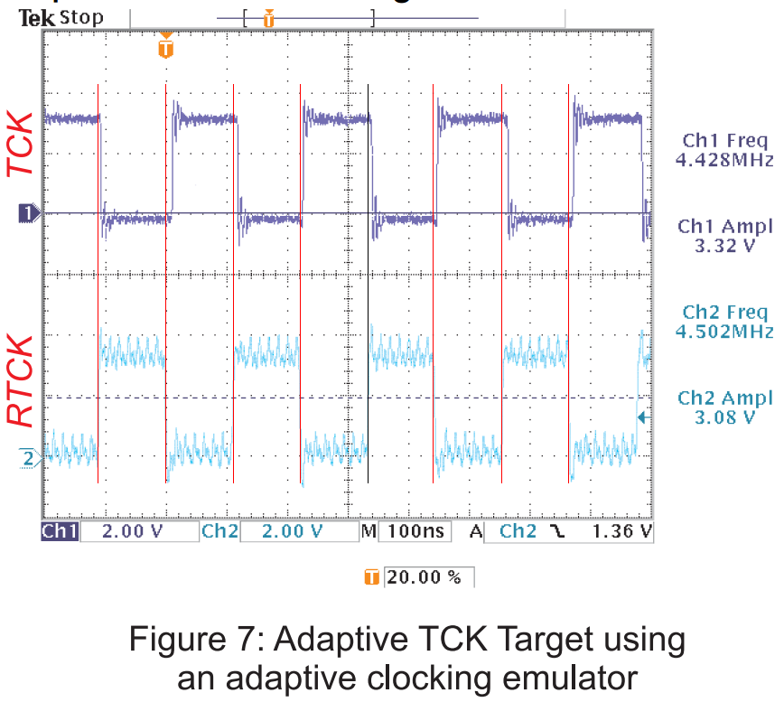
Figure 7 shows the correct operation, which was achieved by attaching the same emulator used in Figure 6 to the same target,
but using an adaptive clocking add-on board.
Now the TCK is throttled by RTCK to meet the requirements of the target.
The JTAG tool waits to detect a falling edge in RTCK before generating the next rising edge in TCK ::
TMS and TDI has clocked to DBGTMS and DBGTDI.
and waits for the rising edge of RTCK to generate the next falling edge in TCK ::
DBGTDO and TDO is valid to be sampled by JTAG Tool.
Conclusion
Maximum JTAG performance and data integrity on today’s TI OMAP platform is subject to handling the adaptive clocking feature of these cores.
The adaptive clocking feature allows for automatic setting of the optimal TCK rate in the system under test.
However, support for this highly useful feature is lacking in JTAG emulators for TI DSPs currently on the market.
Our goal was to correct this deficiency, both by directly incorporating the adaptive clocking logic into Blackhawk™ JTAG emulators
and by developing an add-on board that allows non-adaptive clocking emulators to handle adaptive clocking,
thereby preserving current investments.
Written by: Boycho Kostadinov, Ivailo Kassamakov, and Nenko Lazarov, Fadata Ltd.
Contributions by: Andrey Kostov, Fadata Ltd. Andrew Ferrari, EWA Technologies, Inc.
*******************************************************************************************************
RTCK, also known as: Adaptive Clocking - What is it?
In digital circuit design it is often refered to as “clock synchronisation” the JTAG interface uses one clock
(TCK or TCLK) operating at some speed, your CPU target is operating at another.
The two clocks are not synchronised, they are “asynchronous”
In order for the two to work together they must be synchronised well enough to work;
JTAG can’t go ten times faster than the CPU, for example. There are 2 basic options:
- Use a special "adaptive clocking" circuit to change the JTAG clock rate to match what the CPU currently supports.
- The JTAG clock must be fixed at some speed that’s enough slower than the CPU clock
that all TMS and TDI transitions can be detected.
Does this really matter?
For some chips and some situations, this is a non-issue, like a 500MHz ARM926 with a 5 MHz JTAG link;
the CPU has no difficulty keeping up with JTAG. Startup sequences are often problematic though,
as are other situations where the CPU clock rate changes (perhaps to save power).
For example, Atmel AT91SAM chips start operation from reset with a 32kHz system clock.
Boot firmware may activate the main oscillator and PLL before switching to a faster clock
(perhaps that 500 MHz ARM926 scenario). If you’re using JTAG to debug that startup sequence,
you must slow the JTAG clock to sometimes 1 to 4kHz. After startup completes, JTAG can use a faster clock.
Consider also debugging a 500MHz ARM926 hand held battery powered device that enters a low power “deep sleep” mode,
at 32kHz CPU clock, between keystrokes unless it has work to do.
When would that 5 MHz JTAG clock be usable?
Solution #1 - A special circuit
In order to make use of this, your CPU, board, and JTAG adapter must all support the RTCK feature. Not all of them support this; keep reading!
The RTCK ("Return TCK") signal in some ARM chips is used to help with this problem.
ARM has a good description of the problem described at this link:
http://www.arm.com/support/faqdev/4170.html [checked 28/nov/2008]. Link title:
“How does the JTAG synchronisation logic work? / how does adaptive clocking work?”.
The nice thing about adaptive clocking is that “battery powered hand held device example” - the adaptiveness works perfectly all the time.
One can set a break point or halt the system in the deep power down code, slow step out until the system speeds up.
Note that adaptive clocking may also need to work at the board level, when a board-level scan chain has multiple chips.
Parallel clock voting schemes are good way to implement this, both within and between chips, and can easily be implemented with a CPLD.
It’s not difficult to have logic fan a module’s input TCK signal out to each TAP in the scan chain,
and then wait until each TAP’s RTCK comes back with the right polarity before changing the output RTCK signal.
Texas Instruments makes some clock voting logic available for free (with no support) in VHDL form;
see http://tiexpressdsp.com/index.php/Adaptive_Clocking
Solution #2 - Always works - but may be slower
Often this is a perfectly acceptable solution.
In most simple terms: Often the JTAG clock must be 1/10 to 1/12 of the target clock speed.
But what that “magic division” is varies depending on the chips on your board.
ARM rule of thumb
Most ARM based systems require an 6:1 division;
ARM11 cores use an 8:1 division.
Xilinx rule of thumb is 1/12 the clock speed.
Note: most full speed FT2232 based JTAG adapters are limited to a maximum of 6MHz.
The ones using USB high speed chips (FT2232H) often support faster clock rates (and adaptive clocking).
You can still debug the ’low power’ situations - you just need to either use a fixed and very slow JTAG clock rate ...
or else manually adjust the clock speed at every step. (Adjusting is painful and tedious, and is not always practical.)
It is however easy to “code your way around it” - i.e.: Cheat a little, have a special debug mode in your application that does a “high power sleep”.
If you are careful - 98% of your problems can be debugged this way.
Note that on ARM you may need to avoid using the wait for interrupt operation in your idle loops even if you don’t otherwise change the CPU clock rate.
That operation gates the CPU clock, and thus the JTAG clock; which prevents JTAG access.
One consequence is not being able to halt cores which are executing that wait for interrupt operation.
To set the JTAG frequency use the command:
# Example: 1.234MHz
adapter_khz 1234
The JTAG clock for synthetic cores (e.g. ARM9xxE-S, ARM11xx) must be synchronized externally to the core clock.
This might be done on-chip or off-chip.
The debugger can be switched to ”RTCK” clock mode which causes it to issue a TCK edge
and to wait for the RTCK (Returned TCK) edge to come back before it progress to the next edge.
Instead of using the ”RTCK” clock mode and RTCK signal the debugger can work with a fix TCK frequency.
Theoretically a maximum of 1/6 (ARM9), 1/8 (ARM11) of the core clock frequency can be reached.
Due to propagation delays and tolerances an even lower TCK frequency must be selected.
A fix TCK clock selection will hardly work if the core clock is not known,
dynamically changed or if a power saving mode switch off the clock for a certain time.
In this cases it is strongly recommended to provide and use RTCK.
ARM recommends the following synchronization logic in the technical reference manuals of the cores:

Using adaptive clocking to synchronize the JTAG port
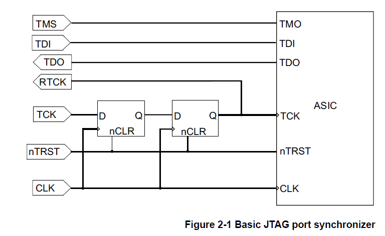
ARM architecture-based devices using only hard macrocells, for example ARM7TDMI® and ARM920T,
use the standard five-wire JTAG interface (TCK, TMS, TDI, TDO, and nTRST).
Some target systems, however, require that JTAG events are synchronized to a clock in the system.
To ensure a valid JTAG CLK setting, these systems often support an extra signal (RTCK) at the JTAG port:
• an Application-Specific Integrated Circuit (ASIC) with single rising-edge D-type design rules, such as one based on an ARM7TDMI-S™ processor
• a system where scan chains external to the ARM macrocell must meet single rising-edge D-type design rules.
The adaptive clocking feature of DSTREAM addresses this requirement.
When adaptive clocking is enabled, DSTREAM issues a TCK signal and waits for the RTCK signal to come back.
DSTREAM does not progress to the next TCK until RTCK is received.
Note
• Adaptive clocking is automatically configured in ARM DS-5™ as required by the target.
• If you use the adaptive clocking feature, transmission delays, gate delays,
and synchronization requirements result in a lower maximum clock frequency than with non-adaptive clocking.
Do not use adaptive clocking unless it is required by the hardware design.
• If, when autoconfiguring a target, the DSTREAM unit receives pulses on RTCK in response to TCK it assumes that adaptive clocking is required,
and enables adaptive clocking in the target configuration. If the hardware does not require adaptive clocking, target is driven slower than it could be.
You can disable adaptive clocking using controls on the JTAG settings dialog box.
• If adaptive clocking is used, DSTREAM cannot detect the clock speed, and therefore cannot scale its internal timeouts.
If the target clock frequency is very slow, a JTAG timeout might occur.
This leaves the JTAG in an unknown state, and DSTREAM cannot operate correctly without reconnecting to the processor.
JTAG timeouts are enabled by default.
You can disable JTAG timeouts by deselecting the option JTAG Timeouts Enabled in the installed RVConfig utility provided with the DSTREAM unit.
You can use adaptive clocking as an interface to targets with slow or widely varying clock frequency,
such as battery-powered equipment that varies its clock speed according to processing demand.
In this system, TCK might be hundreds of times faster than the system clock, and the debugger loses synchronization with the target system.
Adaptive clocking ensures that the JTAG port speed automatically adapts to slow system speed.
The following figure shows a circuit for a basic JTAG port synchronizer.
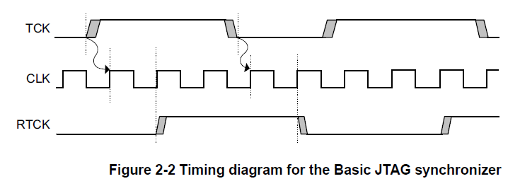
The following figure shows a partial timing diagram for the basic JTAG synchronizer.
The delay can be reduced by clocking the flip-flops from opposite edges of the system clock,
because the second flip-flop only provides better immunity to metastability problems.
Even a single flip-flop synchronizer never completely misses TCK events, because RTCK is part of a feedback loop controlling TCK.
It is common for an ASIC design flow and its design rules to impose a restriction that all flip-flops in a design are clocked by one edge of a single clock.
To interface this to a JTAG port that is completely asynchronous to the system, it is necessary
to convert the JTAG TCK events into clock enables for this single clock,
and to ensure that the JTAG port cannot overrun this synchronization delay.
The following figure shows one possible implementation of this circuit.
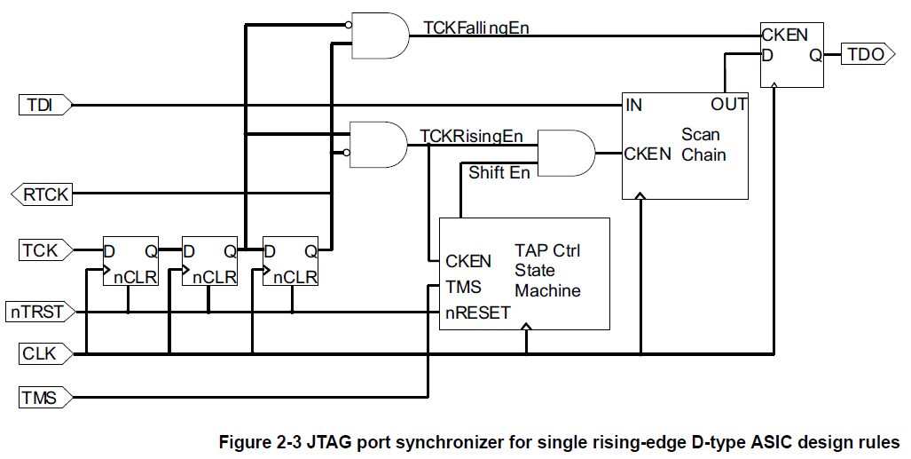
The following figure shows a corresponding partial timing diagram, and how TCKFallingEn and TCKRisingEn
are each active for exactly one period of CLK.
It also shows how these enable signals gate the RTCK and TDO signals so that they only change state at the edges of TCK.