
STM32定时器级联 -- AN2592


Master configuration
When a timer is selected as a master timer, the corresponding trigger output signal
is used by the slave internal trigger (when configured).
The trigger output can be selected from the following list:
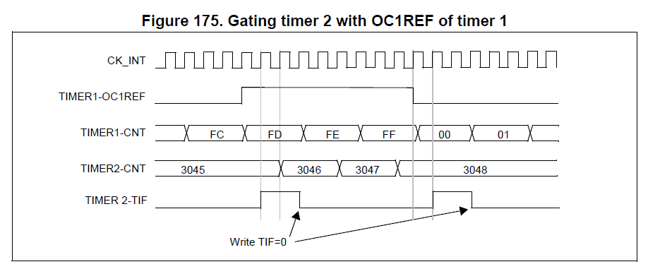
Reset: the UG bit from the EGR register is used as a trigger output (TRGO).
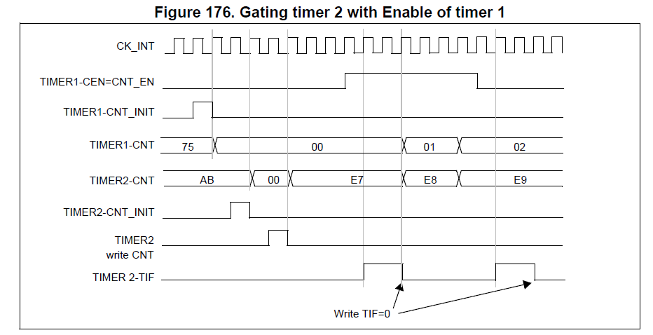
Enable: the counter enable signal is used as a trigger output (TRGO).
It is used to start several timers at the same time, or to control a window in which a slave timer is enabled.
Update: the update event is selected as trigger output (TRGO).
For example, a master timer can be used as a prescaler for a slave timer.
Compare pulse: the trigger output sends a positive pulse
when the CC1IF flag is to be set (even if it was already high) as soon as a capture or a compare match occurs.
OC1Ref: OC1REF signal is used as trigger output (TRGO).
OC2Ref: OC2REF signal is used as trigger output (TRGO).
OC3Ref: OC3REF signal is used as trigger output (TRGO).
OC4Ref: OC4REF signal is used as trigger output (TRGO).
To configure a timer in master mode:
1. Configure your timer.
2. Select the trigger output to be used, by writing the MSM (Master Mode Selection) bits in CR2 register.
3. Enable the MSM (Master/slave mode) bit in the SMCR register to allow a perfect synchronization
between the current timer and its slaves (through TRGO).
For the STM32F30x and STM32F3x8 the timer can generate two trigger outputs,
TRGO2 (used for TIM and ADC synchronization) which can be selected from the following list:
Reset - the UG bit from the EGR register is used as trigger output (TRGO2).
Enable - the Counter Enable signal CNT_EN is used as trigger output (TRGO2).
It is useful to start several timers at the same time or to control a window in which a slave timer is enable.
The Counter Enable signal is generated by a logic OR between CEN control bit and the trigger input when configured in gated mode.
Update - The update event is selected as trigger output (TRGO2).
For instance a master timer can then be used as a prescaler for a slave timer.
Compare Pulse - The trigger output send a positive pulse when the CC1IF flag is to be set (even if it was already high),
as soon as a capture or a compare match occurred.
Compare - OC1REF signal is used as trigger output (TRGO2)
Compare - OC2REF signal is used as trigger output (TRGO2)
Compare - OC3REF signal is used as trigger output (TRGO2)
Compare - OC4REF signal is used as trigger output (TRGO2)
Compare - OC5REF signal is used as trigger output (TRGO2)
Compare - OC6REF signal is used as trigger output (TRGO2)
Compare Pulse - OC4REF rising or falling edges generate pulses on TRGO2
Compare Pulse - OC6REF rising or falling edges generate pulses on TRGO2
Compare Pulse - OC4REF rising or OC6REF rising edges generate pulses on TRGO2
Compare Pulse - OC4REF rising or OC6REF falling edges generate pulses on TRGO2
Compare Pulse - OC5REF rising or OC6REF rising edges generate pulses on TRGO2
Compare Pulse - OC5REF rising or OC6REF falling edges generate pulses on TRGO2
Slave configuration
The slave timer is connected to the master timer through the input trigger.
Each ITRx is connected internally to another timer, and this connection is specific for each STM32 product.
The slave mode can be:
Reset mode: rising edge of the selected trigger input (TRGI)
reinitializes the counter and generates an update of the registers.
Gated mode: the counter clock is enabled when the trigger input (TRGI) is high.
The counter stops (but is not reset) as soon as the trigger becomes low.
Both start and stop of the counter are controlled.
Trigger mode: the counter starts at a rising edge of the trigger TRGI (but it is not reset).
Only the start of the counter is controlled.
External clock mode 1: rising edges of the selected trigger (TRGI) clock the counter.
Combined Reset + Trigger Mode - Rising edge of the selected trigger input (TRGI) reinitializes the counter,
generates an update of the registers and starts the counter.
This mode is present only for STM32F30xC/Bx and STM32F358xC.
To configure a timer in slave mode:
1. Select the slave mode to be used by writing SMS (Slave Mode Selection) bits in SMCR register.
2. Select the internal trigger to be used by writing TS (Trigger selection) bits in SMCR register
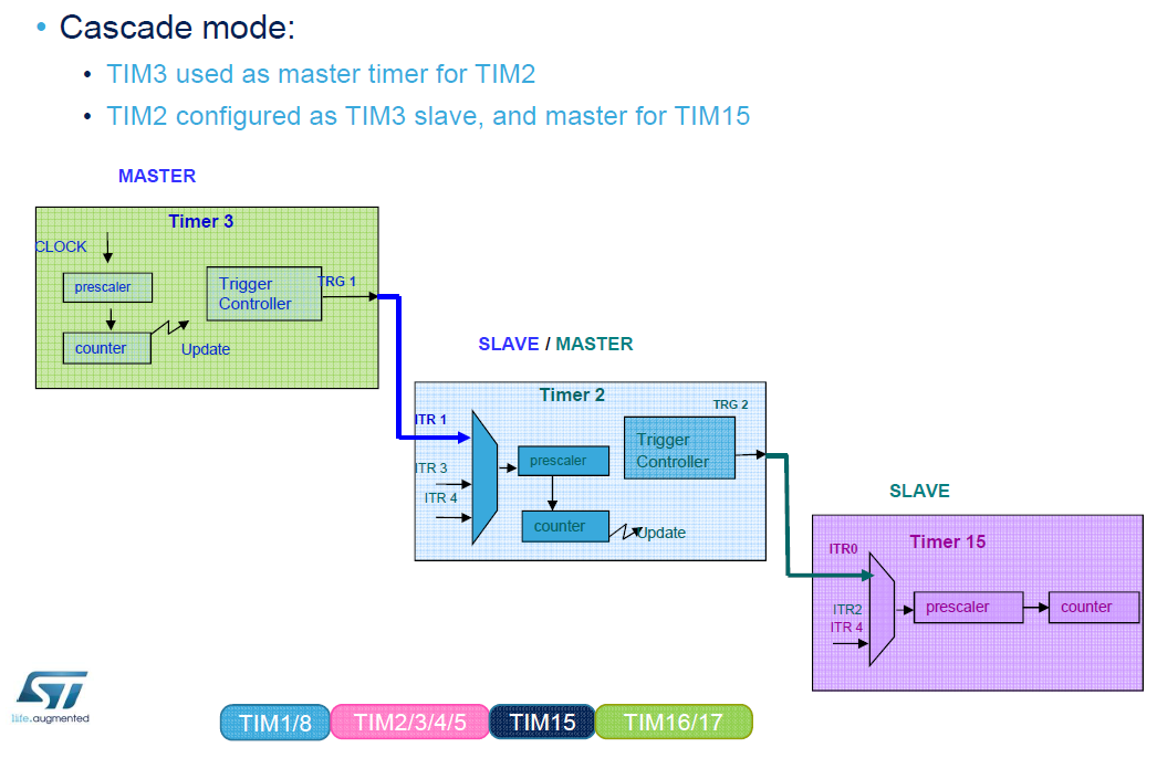
Using one timer as prescaler for another timer
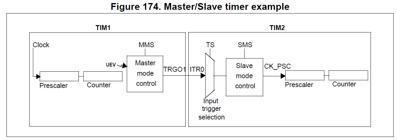
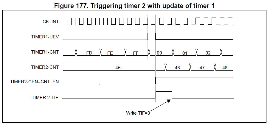
For example, you can configure Timer 1 to act as a prescaler for Timer 2. Refer to Figure 174. To do this:
Configure Timer 1 in master mode so that it outputs a periodic trigger signal on each update event UEV.
If you write MMS=010 in the TIM1_CR2 register, a rising edge is output on TRGO1 each time an update event is generated.
010 : Update - The update event is selected as trigger output (TRGO).
For instance a master timer can then be used as a prescaler for a slave timer.
To connect the TRGO1 output of Timer 1 to Timer 2, Timer 2 must be configured in slave mode using ITR0 as internal trigger.
You select this through the TS bits in the TIM2_SMCR register (writing TS=000).
TS[2:0]: Trigger selection : This bit-field selects the trigger input to be used to synchronize the counter.
000: Internal Trigger 0 (ITR0)
Then you put the slave mode controller in external clock mode 1 (write SMS=111 in the TIM2_SMCR register).
This causes Timer 2 to be clocked by the rising edge of the periodic Timer 1 trigger signal (which correspond to the timer 1 counter overflow).
111: External Clock Mode 1 - Rising edges of the selected trigger (TRGI) clock the counter.
Finally both timers must be enabled by setting their respective CEN bits (TIMx_CR1 register).
Note: If OCx is selected on Timer 1 as trigger output (MMS=1xx), its rising edge is used to clock the counter of timer 2.
100: Compare - OC1REF signal is used as trigger output (TRGO)
101: Compare - OC2REF signal is used as trigger output (TRGO)
110: Compare - OC3REF signal is used as trigger output (TRGO)
111: Compare - OC4REF signal is used as trigger output (TRGO)
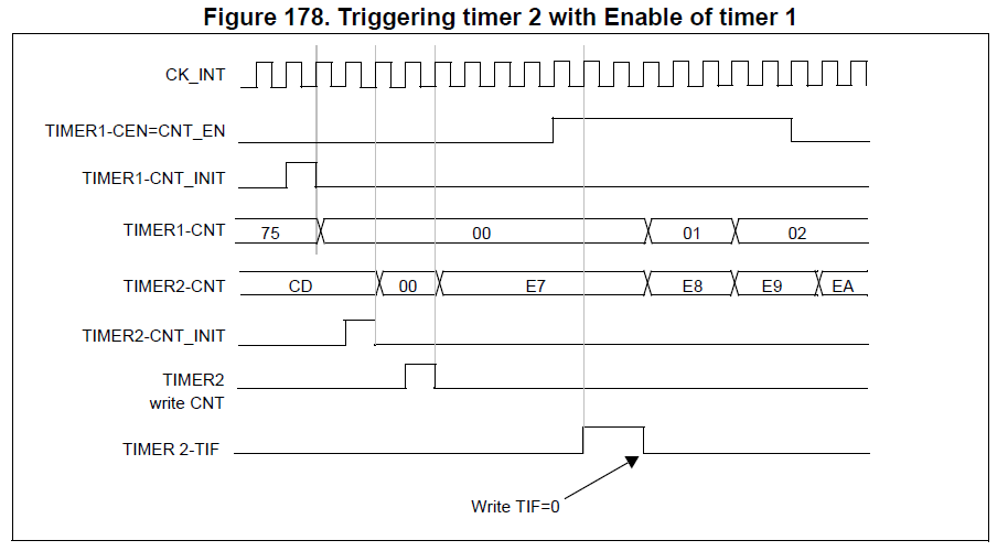
Using one timer to enable another timer
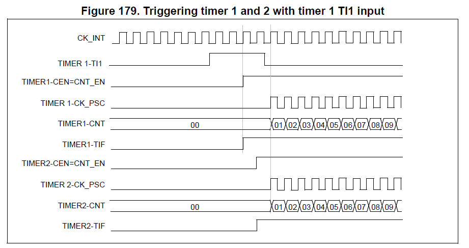
Using one timer to start another timer
Starting 2 timers synchronously in response to an external trigger
STM32的通用定时器可以实现很多功能,例如:定时计数、测量外部信号脉冲宽度、产生PWM波形、测量输入的PWM波形等。
在所有这些操作中,定时器的位数主要影响两个参数,一个是定时或测量的精度,另一个是定时的时间长度。
下面我们以一个列表看一下定时的精度和定时的长度有多少:
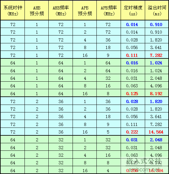
关于各个预分频器的作用请参考下图的右半部分:

从表中可以看出,在最高精度下(14ns)定时长度只有0.91ms,在精度为250ns(即4MHz)时定时长度可达16.38ms。这是仅使用了定时器的独立工作模式的情况。
对于需要高精度并且长延时的应用,16位的定时(上述精度和时间长度)就不够了,这个问题可以有两种解决办法;
第一个办法是通过软件的接力完成,这个方法的可行性在于定时时间较长,允许软件有足够的时间介入计数,这种办法非常方便,多数情况都可使用。
第二种办法是使用STM32特有的定时器级联功能,实现32位的计数效果,因为级联是由硬件触发的,当设置好各项寄存器后,软件不必中途干预,
可以达到高精度长延时的要求。进一步地,STM32最多有四个定时器,如果串联起来,甚至可以实现4*16=64位的计数效果。
简单地说级联功能,即是一个定时器的定时条件满足后,可以产生一个触发信号启动另一个定时器的定时操作。
在ST的网站上有一个应用笔记和对应的例子程序,详细说明和演示了如何使用STM32的级联功能实现32位的输入捕获和32位的输出比较功能,各位可以研究一下:
应用笔记下载地址:http://www.st.com/stonline/products/literature/an/13711.pdf
演示程序下载地址:http://www.st.com/stonline/products/support/micro/files/an2592.zip
这是该应用笔记的摘要:
【AN2592 如何使用STM32F101xx和STM32F103xx的时钟链接功能实现定时器的32位精度】 (2007年8月)
许多应用需要32位的精度,用于测量超过几百秒的外部信号的周期并产生延迟或较大间隔的周期信号。
STM32F101xx和STM32F103xx提供了链接两个16位定时器借以获得32位精度的能力,这是使用了定时器的一种特殊配置和链接机制。
本文给出了模拟一个32位定时器的基本原则;介绍了两个基本的操作模式:
输入捕获模式和输出比较模式。每个模式都是单独介绍并附有实例。
Introduction In many applications, 32-bit resolution is required to measure external signal periods of up to several hundreds of seconds or,
to generate delays or periodic signals with large periods.
The STM32F10x and STM32L15x microcontrollers offer the possibility of chaining two 16-bit timers
to obtain a 32-bit resolution based on a specific configuration of the timers and on the use of the timer link system.
This application note gives general guidelines to emulate a 32-bit timer.
The two basic operating modes are presented:
the input capture mode and the output compare mode.
Each mode is treated independently and, each time, examples of applications are provided
STM32F10x and STM32L15x timer synchronization
1.1 Timer link system presentation
In the STM32F10x and STM32L15x microcontrollers, the embedded timers can be linked together for timer synchronization or chaining purposes.
Using the timer link system, a timer configured in Master mode can:
• reset the counter of the slave timer
• start and/or stop the slave timer counter
• clock the slave timer counter.
1.2 How to synchronize two timers using the link system
In addition to the TIMx_CHx pins, timers have several internal triggers that are indispensable for linking and chaining operation.
Figure 1 shows a simplified representation of the timer block, that highlights the internal triggers.
TIM2 is used as an example. Figure 1. Simplified TIM2 trigger controller block
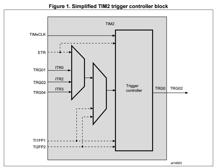
The internal triggers (ITR0, ITR2 and ITR3) are used when TIM2 is configured in the Slave mode.
They then determine which master controls TIM2.
For example, if TIM2 uses ITR2 as an internal trigger, this means that TIM2 is synchronized with TIM3.
These triggers can be easily redirected to the master by setting the right combination of TS bits in the SMCR register.
The trigger output, TRGO, is used when TIM2 is configured in the Master mode.
It then determines which events or signals are sent to the slave timers for synchronization.
Different events or signals can be transmitted to the slave, as listed below.
They are selected using the MMS bits in the CR2 register.
• reset event
• enable event
• update event
• compare pulse
• OCxREF where x is 1, 2, 3 or 4.
Once the master trigger output, TRGO, and the slave’s internal triggers, ITRx, are configured, the two timers are chained.
Four different slave modes can be selected using the SMS bits in the SMCR register:
• Reset mode: the rising edge of the trigger signal reinitializes the counter and generates an update of the registers.
• Gated mode: the slave counter start and stop are both controlled by the high level on the trigger input.
• Trigger mode: the start of the slave counter is controlled by the rising edge of the trigger input signal.
• External clock mode1: the slave counter is clocked by the rising edges of the selected trigger input signal.
32-bit input capture timer resolution
2.1 Principle
To measure the period of an external signal, the timer can be used in input capture mode.
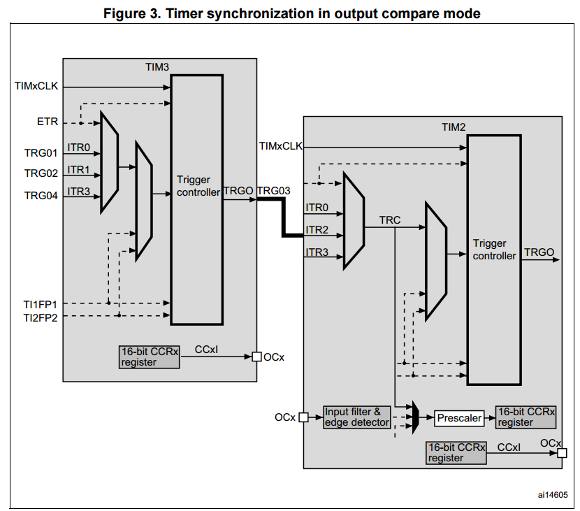
The frequency range that can be measured with the 16-bit timer depends on the TIMxCLK signal.
For example, if the timer of an STM32F10x is clocked by 72 MHz (TIMxCLK = 72 MHz),
the minimum frequency F that can be measured is:
In some applications, the user needs to measure large periods.
The idea is to increase the timer resolution from 16-bit to 32-bit using a specific configuration based on the timer link system.
2.2 Timer configuration
The measure is performed by two timers synchronized in a specific mode.
The master measures the LSB part of the external signal period/frequency
and the slave measures the MSB part.
The two timers are used in input capture mode.
Figure 2 further explains the typical internal connection of the master and slave timers.
TIM3 is used as the master for the TIM2 timer.
2.2.1 TIM3 master configuration
The master timer is used to measure the LSB part of the external period or frequency.
To do so, it is configured as follows:
• no prescaler is used
• the external signal is connected to channel 1 and the rising edge is configured as the active edge.
The input capture module is used to latch the value of the counter
after a transition detected by the corresponding input channel.
To get the external signal period, two consecutive captures are needed
and the period is calculated by subtracting these two values.
To avoid this method and facilitate the input capture measurement,
the master counter is reset after each rising edge detected on the timer input channel by:
• selecting TI1FP1 as the input trigger by setting the TS bits in the SMCR register
• selecting the reset mode as the slave mode by configuring the SMS bits in the SMCR register.
Using this configuration, when an edge is detected, the counter is reset
and the period of the external signal is automatically given by the value on the CCR1 register.
2.2.2 TIM2 slave configuration
The slave timer is used to measure the MSB part of the external frequency.
To do so, it is configured as follows:
• prescaler is fixed to 0xFFFF
• the external signal is connected to channel 1
and the rising edge is configured as the active edge.
2.2.3 Master and slave synchronization
Master configuration
• Use the master update event as the master trigger output (TRGO).
• Enable the Master/Slave mode.
Slave configuration
• Select the slave input trigger: the master trigger output (TRGO) used as the input trigger for the slave.
• Enable the Master/Slave mode.
• Use the external clock mode 1 as the Slave mode:
the slave is clocked by the update event of the master timer.
That is, when the master counter is overflow, the slave counter is incremented.
Using this configuration, each time the period to be measured exceeds the 16-bit master timer Auto-reload register,
an update event is generated to clock the slave timer.
When the active edge is detected on the master and slave timer inputs,
the two counter values are copied into the master CCR1 register and the slave CCR1 register, respectively.
Since the slave is clocked by the master update event, the number of master overflow
is recorded by the slave as the MSB part of the 32-bit input capture register;
the LSB is read on the Master CCR1.
The external signal frequency is calculated on each master input capture interrupt as follows:

LSB is the master capture compare register value (LSB = TIM3->CCR1 register value).
To get the MSB value, two consecutive captures are needed
and the MSB variable is calculated by subtracting these two values as shown below:
If MSB1 > MSB2 then MSB = 0xFFFF – ((MSB1 – MSB2)) – 1
If MSB1 < MSB2 then MSB = (MSB2 – MSB1) – 1
MSB1 and MSB2 are given by the slave capture compare value (TIM2->CCR2 register value).
Since the master timer is used in Reset mode,
when the active edge is detected on the master timer,
the counter is reinitialized and an update is generated.
To avoid this additional update event, 1 is subtracted from the MSB value.
Using this method, the lowest frequency that can be measured on STM32F10x,
with TIMxCLK equal to 72 MHz, is 0.017 Hz instead of 1098 Hz when a 16-bit timer is used.
TIMxCLK 等于72 MHz的情况下,这种方法可以测量的最小频率是0.017Hz, (也就是0.017Hz,刚好是72MHz/2^32),
而不是用16bit定时计数器时所能测量的最小频率1096Hz了,(刚好也是72MHz/2^16)
/* Private define ------------------------------------------------------------*/
/* Private macro -------------------------------------------------------------*/
/* Private variables ---------------------------------------------------------*/
TIM_TimeBaseInitTypeDef  TIM_TimeBaseStructure;
TIM_ICInitTypeDef  TIM_ICInitStructure;
TIM_OCInitTypeDef TIM_OCInitStructure;

/* Private function prototypes -----------------------------------------------*/
void RCC_Configuration(void);
void GPIO_Configuration(void);
void NVIC_Configuration(void);

/* Private functions ---------------------------------------------------------*/

/**
  * @brief  Main program
  * @param  None
  * @retval : None
  */
int main(void)
{
  /* System Clocks Configuration */
  RCC_Configuration();

  /* NVIC Configuration */
  NVIC_Configuration();

  /* GPIO Configuration */
  GPIO_Configuration();

/*---------------------------- TIM2 Configuration ----------------------------*/
  /* Time base configuration */
  TIM_TimeBaseStructure.TIM_Period = 65535;
  TIM_TimeBaseStructure.TIM_Prescaler = 0;
  TIM_TimeBaseStructure.TIM_ClockDivision = 0;
  TIM_TimeBaseStructure.TIM_CounterMode = TIM_CounterMode_Up;

  TIM_TimeBaseInit(TIM2, &TIM_TimeBaseStructure);

  TIM_PrescalerConfig(TIM2, 65535, TIM_PSCReloadMode_Update);

  /* TIM2 Input Capture configuration */
  TIM_ICInitStructure.TIM_Channel = TIM_Channel_1;
  TIM_ICInitStructure.TIM_ICPolarity = TIM_ICPolarity_Rising;
  TIM_ICInitStructure.TIM_ICSelection = TIM_ICSelection_DirectTI;
  TIM_ICInitStructure.TIM_ICPrescaler = TIM_ICPSC_DIV1;
  TIM_ICInitStructure.TIM_ICFilter = 0;

  TIM_ICInit(TIM2, &TIM_ICInitStructure);

  /* Disable the TIM2 Update event */
  TIM_UpdateDisableConfig(TIM2, ENABLE);

  /* ----------------------TIM2 Configuration as slave for the TIM3 ----------*/
  /* Select the TIM2 Input Trigger: TIM3 TRGO used as Input Trigger for TIM2*/
  TIM_SelectInputTrigger(TIM2, TIM_TS_ITR2);
  /* Use the External Clock as TIM2 Slave Mode */
  TIM_SelectSlaveMode(TIM2, TIM_SlaveMode_External1);
  /* Enable the TIM2 Master Slave Mode */
  TIM_SelectMasterSlaveMode(TIM2, TIM_MasterSlaveMode_Enable);

/*---------------------------- TIM3 Configuration ----------------------------*/
  /* Time base configuration */
  TIM_TimeBaseStructure.TIM_Period = 65535;
  TIM_TimeBaseStructure.TIM_Prescaler = 0;
  TIM_TimeBaseStructure.TIM_ClockDivision = 0;
  TIM_TimeBaseStructure.TIM_CounterMode = TIM_CounterMode_Up;

  TIM_TimeBaseInit(TIM3, &TIM_TimeBaseStructure);

/* TIM3: Master Configuration: Input Capture Mode */
  TIM_ICInitStructure.TIM_Channel = TIM_Channel_1;
  TIM_ICInitStructure.TIM_ICPolarity = TIM_ICPolarity_Rising;
  TIM_ICInitStructure.TIM_ICSelection = TIM_ICSelection_DirectTI;
  TIM_ICInitStructure.TIM_ICPrescaler = TIM_ICPSC_DIV1;
  TIM_ICInitStructure.TIM_ICFilter = 0;

  TIM_ICInit(TIM3, &TIM_ICInitStructure);

/* TIM3 Configuration to reset counter after each Rising edge detected on TI1*/
  TIM_SelectInputTrigger(TIM3, TIM_TS_TI1FP1);

  TIM_SelectSlaveMode(TIM3, TIM_SlaveMode_Reset);

  TIM_UpdateRequestConfig(TIM3, TIM_UpdateSource_Regular);

/* ----------------------TIM3 Configuration as Master for the TIM2 -----------*/
  /* Use the TIM3 Update event  as TIM3 Trigger Output(TRGO) */
  TIM_SelectOutputTrigger(TIM3, TIM_TRGOSource_Update);
  /* Enable the TIM3 Master Slave Mode */
  TIM_SelectMasterSlaveMode(TIM3, TIM_MasterSlaveMode_Enable);

  /* Enable the TIM3 CC1 Interrupt */
  TIM_ITConfig(TIM3, TIM_IT_CC1, ENABLE);

  /* Enable TIM3 and TIM2 counters */
  TIM_Cmd(TIM3, ENABLE);
  TIM_Cmd(TIM2, ENABLE);

  while (1)
  {
  }
}

/**
  * @brief  Configures the different system clocks.
  * @param  None
  * @retval : None
  */
void RCC_Configuration(void)
{
  /* Setup STM32 system (clock, PLL and Flash configuration) */
  SystemInit();

  /* TIM2 and TIM3 clock enable */
  RCC_APB1PeriphClockCmd(RCC_APB1Periph_TIM2 | RCC_APB1Periph_TIM3, ENABLE);

  /* GPIOA clock enable */
  RCC_APB2PeriphClockCmd(RCC_APB2Periph_GPIOA, ENABLE);
}

/**
  * @brief  Configures NVIC and Vector Table base location.
  * @param  None
  * @retval : None
  */
void NVIC_Configuration(void)
{
  NVIC_InitTypeDef NVIC_InitStructure;

  NVIC_InitStructure.NVIC_IRQChannel = TIM3_IRQn;
  NVIC_InitStructure.NVIC_IRQChannelPreemptionPriority = 0;
  NVIC_InitStructure.NVIC_IRQChannelSubPriority = 0;
  NVIC_InitStructure.NVIC_IRQChannelCmd = ENABLE;
  NVIC_Init(&NVIC_InitStructure);
}

/**
  * @brief  Configure the TIM2 and TIM3 Pins.
  * @param  None
  * @retval : None
  */
void GPIO_Configuration(void)
{
  GPIO_InitTypeDef GPIO_InitStructure;

  /* GPIOA Configuration:TIM2 and TIM3 Channel1 in Input */
  GPIO_InitStructure.GPIO_Pin = GPIO_Pin_0 | GPIO_Pin_6;
  GPIO_InitStructure.GPIO_Mode = GPIO_Mode_IN_FLOATING;

  GPIO_Init(GPIOA, &GPIO_InitStructure);
}
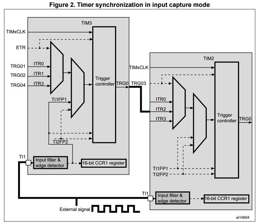
32-bit output compare timer resolution
3.1 Principle and timer configuration
The idea is to use two timers to generate a 32-bit resolution output compare signal;
one timer that gives the MSB, and the other that provides the LSB of the 32-bit output compare signal.
Compare pulse is one of the master modes offered by the STM32 timers.
With the Compare pulse mode selected, each time the CC1IF flag is to be set,
that is, as soon as there is a compare match, the master trigger output (TRGO) sends a positive pulse.
In addition, if the timer master is being used in output compare mode,
the LSB or MSB part of the 32-bit output compare signal is loaded into the master CCRx register.
When the counter of the master reaches the loaded value, it triggers the other timer,
causing it to generate the missing MSB or LSB.
To generate the MSB or the LSB part of the output compare signal,
the slave timer must wait for the master trigger output signal and then start counting
in order to introduce the missing 16-bit (LSB or MSB) part.
For this, the slave timer has to be configured in the one-pulse mode (OPM).
The one-pulse mode is a particular case of the input capture and output compare modes.
It allows the counter to be started in response to a stimulus,
and to generate a pulse with a programmable length after a programmable delay.
The counter start can be controlled through the slave mode controller
and the waveform can be generated in output compare mode.
If the one-pulse mode (OPM) is selected by setting the OPM bit in the CR1 register,
the counter stops automatically at the next update event.
The STM32 timers offer the possibility of redirecting the internal trigger (ITR)
and of using it as the input signal for the capture/compare array.
In this case, the internal trigger can be used as a stimulus for a slave timer initially configured in one-pulse mode (OPM).
This is done by configuring the CCxS bits in the CCMRx register to be mapped on TRC.
This configuration allows the cascading of two timers to obtain a 32-bit time base resolution.
Figure 3 explains how the two timers are cascaded.
TIM3 is the master timer used in output compare mode; the trigger output (TRGO3)
sends a positive pulse when the CC1IF flag is to be set as soon as a compare match occurs.
To connect the TRGO3 output of TIM3 to TIM2,
TIM2 must be configured in slave mode using ITR2 as the internal trigger.
Then the slave mode controller is configured in trigger mode.
This causes the TIM2 counter to be started at a rising edge of the TIM3 trigger signal (that corresponds to the TIM3 compare match).
The two timers are configured as described below.
TIM3 master configuration
• configure TIM3 in output compare mode, the CCRx register must be loaded with the LSB or the MSB part of the signal
• use the timer master compare pulse event as the trigger output (TRGO)
• set the prescaler value
• enable the master/slave mode.
TIM2 slave configuration
• TIM2 is used in one-pulse mode, so there are three steps of configuration:
– the input capture module
– the output compare module and the trigger controller
– and the synchronization part.
• to configure the TIM2 timer, the user has to:
– map TRC onto TIx by writing CCxS = '11' into the TIMx_CCMRx register
– configure ITR2 as the trigger for the slave mode controller (TRGI) by writing TS = '010' in the TIMx_SMCR register
– use the trigger mode as the slave mode by writing SMS to '110' in the TIMx_SMCR register: the counter start is controlled by the master
– configure the output compare mode by setting the right combination of the OCxM bits in the TIMx_CCMRx register
(OCxM can be set to '000', '001', '010' or '011'). The CCRx register must be loaded with the MSB or the LSB part
– set the prescaler value
– select the output pin by configuring the CCxS bits in the TIMx_CCMRx register
– enable the one-pulse mode by setting the OPM bit in the TIMx_CR1 register.
This causes the counter to stop at the next update event.
So the counter start is controlled by the master but the stop is controlled by the counter itself.
3.2 Output compare mode configuration
3.2.1 Output compare active mode example
The following example is calculated for STM32F10x.
Therefore, the maximum clock frequency is considered as 72 MHz.
For STM32L1xx, 32 MHz has to be used instead.
Master configuration
TIM3 is used as the master timer in output compare active mode.
For STM32F10x, TIM3CLK is equal to 72 MHz, no prescaler is used, so the TIM3 counter clock is equal to:
TIM3 counter clock = TIM3CLK/(prescaler + 1) = 72 MHz
TIM3 generates the LSB part of the 32-bit output compare delay, and this delay value is loaded into the CCR1 register.
Slave configuration
TIM2 is used as the slave timer in one-pulse mode as described below:
• channel1, channel2 and channel3 are used in output compare active mode. The corresponding CCRx registers are loaded with the MSB part
• channel4 is used in input capture mode: CC4S is connected to TRC
• the prescaler is set to 0xFFFF
• the trigger mode is used as the slave mode TIM2 is a slave for TIM3
so ITR2 is used as the internal trigger (TS = ‘010’ in TIM2_SMCR register).
In one-pulse mode, the edge detection on TIM2 IC4 (TRC) sets the TIM2 counter enable (CEN) bit,
which enables the counter.
When a match is found between the capture/compare register and the counter,
the output compare function assigns the corresponding output pin with a programmable value
determined by the output compare mode and the output polarity.
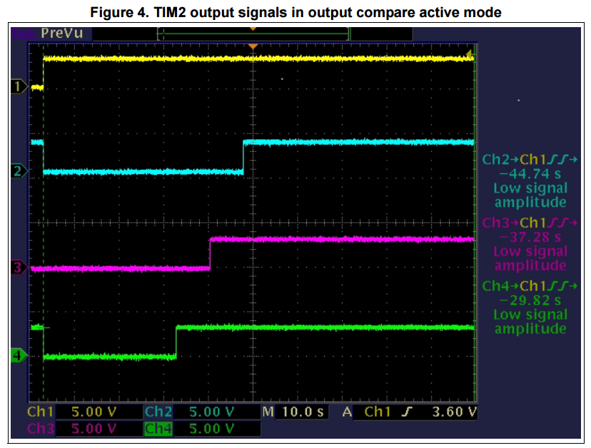
In this example, after the programmed delays, the TIM2 pins are set to their active mode.
In this example, the three capture compare register values are
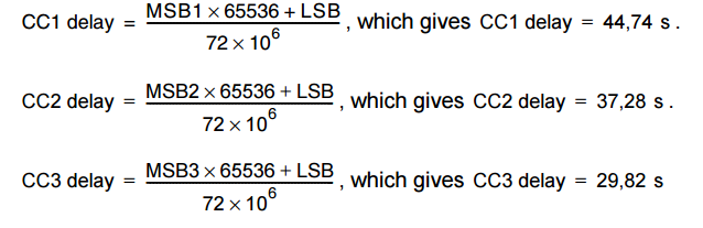
TIM2_CCR1 = MSB1 = 0xC000, TIM2_CCR2 = MSB2 = 0xA000 and TIM2_CCR3 = MSB3 = 0x8000, respectively.
TIM3_CCR1 = LSB = 0x8534. The equations of the TIM2 output compare delays are given below and shown in Figure 4.
Note:
The same configuration steps are used for the output compare inactive mode.
The user only needs to place TIM2 in output compare inactive mode instead of output compare active mode,
and then to go through the same steps. Figure 4 shows the three signals.
/* Includes ------------------------------------------------------------------*/
#include "stm32f10x.h"

/* Private typedef -----------------------------------------------------------*/
/* Private define ------------------------------------------------------------*/
/* Private macro -------------------------------------------------------------*/
/* Private variables ---------------------------------------------------------*/
TIM_TimeBaseInitTypeDef  TIM_TimeBaseStructure;
TIM_OCInitTypeDef  TIM_OCInitStructure;
TIM_ICInitTypeDef TIM_ICInitStructure;
uint16_t MSB1 = 49152;
uint16_t MSB2 = 40960;
uint16_t MSB3 = 32768;
uint16_t LSB = 34100;

/* Private function prototypes -----------------------------------------------*/
void RCC_Configuration(void);
void GPIO_Configuration(void);

/* Private functions ---------------------------------------------------------*/

/**
  * @brief  Main program
  * @param  None
  * @retval : None
  */
int main(void)
{
  /* System Clocks Configuration */
  RCC_Configuration();

  /* GPIO Configuration */
  GPIO_Configuration();

  /* ---------------------------------------------------------------
  TIM2 and TIM3 synchronisation configuration:
  1/ TIM2 is configured to be used as slave for the TIM3.
  2/ TIM2 is used in One Pulse Mode: at each pulse received on its input, a
     pulse will be generated after the delay loaded in the corresponding
     registers (TIM2_CCRx).
  3/ TIM3 generates the input signal for TIM2. TIM3 OC1 signal  is used as
     Trigger Output(TRGO), this event will trigger the slave Timer (TIM2)
     counter, so the slave mode is the Trigger mode.

  TIM3 Configuration:
  - Output Compare Active Mode: the TIM3 delay is the LSB part of the TIM2 output
    signal.
  - TIM3CLK = 72MHz
  - Prescaler = 0

  TIM2 Configuration:
  - Output Compare Active Mode: the TIM2 delays are the MSB parts of the TIM2
    output signals.
  - TIM2CLK = 72MHz
  - Prescaler = 65535

  TIM2 Output Compare delays compute:

  CC1 delay = (MSB1*65535 + LSB) / TIM2CLK
            = 44.74 s

  CC2 delay = (MSB2*65535 + LSB) / TIM2CLK
            = 37.28 s

  CC3 delay = (MSB3*65535 + LSB) / TIM2CLK
            = 29.82 s
--------------------------------------------------------------- */
  /* Reference signal set to Low level */
  GPIO_ResetBits(GPIOB, GPIO_Pin_0);

  /* TIM2 Time base configuration */
  TIM_TimeBaseStructure.TIM_Period = 65535;
  TIM_TimeBaseStructure.TIM_Prescaler = 65535;
  TIM_TimeBaseStructure.TIM_ClockDivision = 0;
  TIM_TimeBaseStructure.TIM_CounterMode = TIM_CounterMode_Up;

  TIM_TimeBaseInit(TIM2, &TIM_TimeBaseStructure);

  /* TIM2 Output Compare Mode configuration: Channel1 */
  TIM_OCInitStructure.TIM_OCMode = TIM_OCMode_Active;
  TIM_OCInitStructure.TIM_OutputState = TIM_OutputState_Enable;
  TIM_OCInitStructure.TIM_OCPolarity = TIM_OCPolarity_Low;
  TIM_OCInitStructure.TIM_Pulse = MSB1;

  TIM_OC1Init(TIM2, &TIM_OCInitStructure);

  /* TIM2 Output Compare Mode configuration: Channel2 */
  TIM_OCInitStructure.TIM_OCMode = TIM_OCMode_Active;
  TIM_OCInitStructure.TIM_OutputState = TIM_OutputState_Enable;
  TIM_OCInitStructure.TIM_OCPolarity = TIM_OCPolarity_Low;
  TIM_OCInitStructure.TIM_Pulse = MSB2;

  TIM_OC2Init(TIM2, &TIM_OCInitStructure);

  /* TIM2 Output Compare Mode configuration: Channel3 */
  TIM_OCInitStructure.TIM_OCMode = TIM_OCMode_Active;
  TIM_OCInitStructure.TIM_OutputState = TIM_OutputState_Enable;
  TIM_OCInitStructure.TIM_OCPolarity = TIM_OCPolarity_Low;
  TIM_OCInitStructure.TIM_Pulse = MSB3;

  TIM_OC3Init(TIM2, &TIM_OCInitStructure);

  /* TIM2 configuration in Input Capture Mode */
  TIM_ICInitStructure.TIM_Channel = TIM_Channel_4;
  TIM_ICInitStructure.TIM_ICPolarity = TIM_ICPolarity_Rising;
  TIM_ICInitStructure.TIM_ICSelection = TIM_ICSelection_TRC;
  TIM_ICInitStructure.TIM_ICPrescaler = TIM_ICPSC_DIV1;
  TIM_ICInitStructure.TIM_ICFilter = 0;

  TIM_ICInit(TIM2, &TIM_ICInitStructure);

  /* One Pulse Mode selection */
  TIM_SelectOnePulseMode(TIM2, TIM_OPMode_Single);

  /* Input Trigger selection */
  TIM_SelectInputTrigger(TIM2, TIM_TS_ITR2);

  /* Slave Mode selection: Trigger Mode */
  TIM_SelectSlaveMode(TIM2, TIM_SlaveMode_Trigger);

  /*---------------------------- TIM3 Configuration --------------------------*/
  /* Time base configuration */
  TIM_TimeBaseStructure.TIM_Period = 65535;
  TIM_TimeBaseStructure.TIM_Prescaler = 0;
  TIM_TimeBaseStructure.TIM_ClockDivision = 0;
  TIM_TimeBaseStructure.TIM_CounterMode = TIM_CounterMode_Up;

  TIM_TimeBaseInit(TIM3, &TIM_TimeBaseStructure);

  /* Output Compare Active Mode configuration: Channel1 */
  TIM_OCInitStructure.TIM_OCMode = TIM_OCMode_Active;
  TIM_OCInitStructure.TIM_OutputState = TIM_OutputState_Enable;
  TIM_OCInitStructure.TIM_OCPolarity = TIM_OCPolarity_Low;
  TIM_OCInitStructure.TIM_Pulse = LSB;

  TIM_OC1Init(TIM3, &TIM_OCInitStructure);

  /* TIM3 OC1 Master Output Trigger selection */
  TIM_SelectOutputTrigger(TIM3, TIM_TRGOSource_OC1);

  /* Reference signal set to High level */
  GPIO_SetBits(GPIOB, GPIO_Pin_0);

  /* TIM3 counter enable */
  TIM_Cmd(TIM3, ENABLE);

  while (1)
  {
  }
}

/**
  * @brief  Configures the different system clocks.
  * @param  None
  * @retval : None
  */
void RCC_Configuration(void)
{
  /* Setup STM32 system (clock, PLL and Flash configuration) */
  SystemInit();

  /* TIM2 and TIM3 clock enable */
  RCC_APB1PeriphClockCmd(RCC_APB1Periph_TIM2 | RCC_APB1Periph_TIM3, ENABLE);

  /* GPIOA and GPIOB clock enable */
  RCC_APB2PeriphClockCmd(RCC_APB2Periph_GPIOA | RCC_APB2Periph_GPIOB, ENABLE);
}

/**
  * @brief  Configures     the TIM2 Pins.
  * @param  None
  * @retval : None
  */
void GPIO_Configuration(void)
{
  GPIO_InitTypeDef GPIO_InitStructure;

/* GPIOA Configuration:TIM2 Channel1, 2 and 3 in Alternate Function push-pull */
  GPIO_InitStructure.GPIO_Pin = GPIO_Pin_0 | GPIO_Pin_1 | GPIO_Pin_2;
  GPIO_InitStructure.GPIO_Mode = GPIO_Mode_AF_PP;
  GPIO_InitStructure.GPIO_Speed = GPIO_Speed_50MHz;

  GPIO_Init(GPIOA, &GPIO_InitStructure);

  /* GPIOB Configuration:Pin0 in Output */
  GPIO_InitStructure.GPIO_Pin = GPIO_Pin_0;
  GPIO_InitStructure.GPIO_Mode = GPIO_Mode_Out_PP;

  GPIO_Init(GPIOB, &GPIO_InitStructure);
}
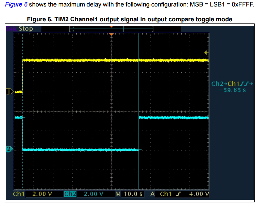
3.2.2 Output compare toggle mode example
The following example is calculated for STM32F10x.
Therefore, the maximum clock frequency is considered as 72 MHz.
For STM32L1xx, 32 MHz has to be used instead.
Master configuration
TIM3 is used as the master timer in output compare toggle mode.
TIM3CLK is equal to 72 MHz. The prescaler is set to 0xFFFF.
TIM3 generates the MSB part of the 32-bit output compare delay, and this delay value is loaded into the CCR1 register.
Slave configuration
TIM2 is used as the slave timer in one-pulse mode as described below:
• channel 1, channel2 and channel3 are used in output compare toggle mode. The corresponding CCRx registers are loaded with the LSB part
• channel4 is used in input capture mode: CC4S is connected to TRC
• the prescaler is set to 0x0
• the trigger mode is used as the slave mode.
TIM2 is a slave for TIM3 so ITR2 is used as the internal trigger (TS = ‘010’ in TIM2_SMCR register).
In one-pulse mode, the edge detection on TIM2 IC4 (TRC) sets the TIM2 counter enable (CEN) bit,
which enables the counter.
When a match is found between the capture/compare register and the counter,
the output compare function assigns the corresponding output pin with a programmable value determined
by the output compare mode and the output polarity.
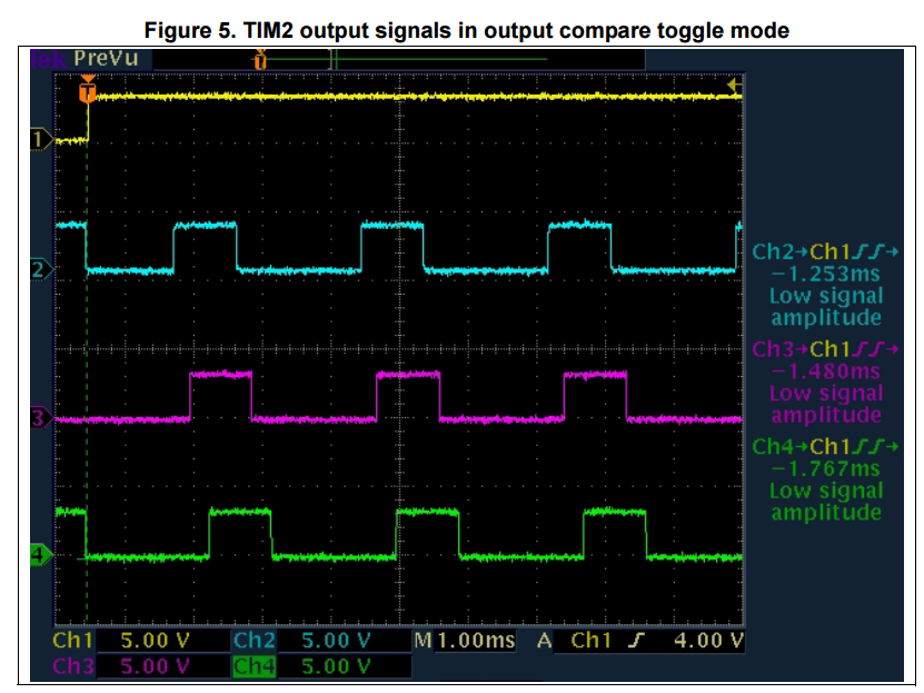
In this example, when the match is found between the counter and the TIM2_CCRx registers,
the TIM2 pins toggle and capture compare interrupts are generated.
In the corresponding routine, the TIM2_CCRx registers are updated in order to
have three periodic signals with three different frequencies.
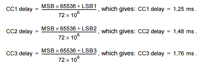
In this example, the three capture compare register values are
TIM2_CCR1 = LSB1 = 0x5FFF,
TIM2_CCR2 = LSB2 = 0x9FFF and
TIM2_CCR3 = LSB3 = 0xEFFF, respectively.
TIM3_CCR1 = MSB = 0x1.
Note:
The same configuration steps are used for the output compare timing mode.
The user only needs to place TIM2 in output compare timing mode instead of output compare toggle mode,
and then to go through the same steps. Figure 5 shows the three signals
/* Includes ------------------------------------------------------------------*/
#include "stm32f10x.h"

/* Private typedef -----------------------------------------------------------*/
/* Private define ------------------------------------------------------------*/
/* Private macro -------------------------------------------------------------*/
/* Private variables ---------------------------------------------------------*/
TIM_TimeBaseInitTypeDef  TIM_TimeBaseStructure;
TIM_OCInitTypeDef  TIM_OCInitStructure;
TIM_ICInitTypeDef TIM_ICInitStructure;
uint16_t LSB1 = 24575;
uint16_t LSB2 = 40959;
uint16_t LSB3 = 61439;
uint16_t MSB = 1;

/* Private function prototypes -----------------------------------------------*/
void RCC_Configuration(void);
void GPIO_Configuration(void);
void NVIC_Configuration(void);

/* Private functions ---------------------------------------------------------*/

/**
  * @brief  Main program
  * @param  None
  * @retval : None
  */
int main(void)
{
  /* System Clocks Configuration */
  RCC_Configuration();

  /* NVIC Configuration */
  NVIC_Configuration();

  /* GPIO Configuration */
  GPIO_Configuration();

 /* ---------------------------------------------------------------
  TIM2 and TIM3 synchronisation configuration:
  1/ TIM2 is configured to be used as slave for the TIM3.
  2/ TIM2 is used in One Pulse Mode: at each pulse received on its input, a pulse
     will be generated after the delay loaded in the corresponding registers
     (TIM2_CCRx).
  3/ TIM3 generates the input signal for TIM2. TIM3 OC1 signal is used as Trigger
     Output(TRGO), this event will trigger the slave Timer (TIM2) counter, so
     the slave mode    is the Trigger mode.

  TIM3 Configuration:
  - Output Compare Active Mode: the TIM3 delay is the MSB part of the TIM2 output
    signal.
  - TIM3CLK = 72MHz
  - Prescaler = 65535

  TIM2 Configuration:
  - Output Compare Active Mode: the TIM2 delays are the LSB parts of the TIM2
    output signals.
  - TIM2CLK = 72MHz
  - Prescaler = 0

  TIM2 Output Compare delays compute:

  CC1 delay = (MSB*65535 + LSB1) / TIM2CLK
            = 1.25 ms

  CC2 delay = (MSB*65535 + LSB2) / TIM2CLK
            = 1.48 ms

  CC3 delay = (MSB*65535 + LSB3) / TIM2CLK
            = 1.76 ms
--------------------------------------------------------------- */

 /* Reference signal set to Low level */
  GPIO_ResetBits(GPIOB, GPIO_Pin_0);

  /* TIM2 Time base configuration */
  TIM_TimeBaseStructure.TIM_Period = 65535;
  TIM_TimeBaseStructure.TIM_Prescaler = 0;
  TIM_TimeBaseStructure.TIM_ClockDivision = 0;
  TIM_TimeBaseStructure.TIM_CounterMode = TIM_CounterMode_Up;

  TIM_TimeBaseInit(TIM2, &TIM_TimeBaseStructure);

  /* TIM2 ouput Toggle Mode configuration: Channel1 */
  TIM_OCInitStructure.TIM_OCMode = TIM_OCMode_Toggle;
  TIM_OCInitStructure.TIM_OutputState = TIM_OutputState_Enable;
  TIM_OCInitStructure.TIM_OCPolarity = TIM_OCPolarity_Low;
  TIM_OCInitStructure.TIM_Pulse = LSB1;

  TIM_OC1Init(TIM2, &TIM_OCInitStructure);

  /* TIM2 ouput Toggle Mode configuration: Channel2 */
  TIM_OCInitStructure.TIM_OCMode = TIM_OCMode_Toggle;
  TIM_OCInitStructure.TIM_OutputState = TIM_OutputState_Enable;
  TIM_OCInitStructure.TIM_OCPolarity = TIM_OCPolarity_Low;
  TIM_OCInitStructure.TIM_Pulse = LSB2;

  TIM_OC2Init(TIM2, &TIM_OCInitStructure);

  /* TIM2 ouput Toggle Mode configuration: Channel3 */
  TIM_OCInitStructure.TIM_OCMode = TIM_OCMode_Toggle;
  TIM_OCInitStructure.TIM_OutputState = TIM_OutputState_Enable;
  TIM_OCInitStructure.TIM_OCPolarity = TIM_OCPolarity_Low;
  TIM_OCInitStructure.TIM_Pulse = LSB3;

  TIM_OC3Init(TIM2, &TIM_OCInitStructure);

  /* TIM2 configuration in Input Capture Mode */
  TIM_ICInitStructure.TIM_Channel = TIM_Channel_4;
  TIM_ICInitStructure.TIM_ICPolarity = TIM_ICPolarity_Rising;
  TIM_ICInitStructure.TIM_ICSelection = TIM_ICSelection_TRC;
  TIM_ICInitStructure.TIM_ICPrescaler = TIM_ICPSC_DIV1;
  TIM_ICInitStructure.TIM_ICFilter = 0;

  TIM_ICInit(TIM2, &TIM_ICInitStructure);

  /* One Pulse Mode selection */
  TIM_SelectOnePulseMode(TIM2, TIM_OPMode_Single);

  /* Slave Mode selection: Trigger Mode */
  TIM_SelectSlaveMode(TIM2, TIM_SlaveMode_Trigger);

  /*---------------------------- TIM3 Configuration --------------------------*/
  /* Time base configuration */
  TIM_TimeBaseStructure.TIM_Period = 65535;
  TIM_TimeBaseStructure.TIM_Prescaler = 65535;
  TIM_TimeBaseStructure.TIM_ClockDivision = 0;
  TIM_TimeBaseStructure.TIM_CounterMode = TIM_CounterMode_Up;

  TIM_TimeBaseInit(TIM3, &TIM_TimeBaseStructure);

  /* Output Compare Toggle Mode configuration: Channel1 */
  TIM_OCInitStructure.TIM_OCMode = TIM_OCMode_Toggle;
  TIM_OCInitStructure.TIM_OutputState = TIM_OutputState_Enable;
  TIM_OCInitStructure.TIM_OCPolarity = TIM_OCPolarity_Low;
  TIM_OCInitStructure.TIM_Pulse = MSB;

  TIM_OC1Init(TIM3, &TIM_OCInitStructure);

  /* TIM3 OC1 Master Output Trigger selection */
  TIM_SelectOutputTrigger(TIM3, TIM_TRGOSource_OC1);

  /* TIM2 Input Trigger selection */
  TIM_SelectInputTrigger(TIM2, TIM_TS_ITR2);

  /* TIM3 CC1 interrupt enable */
  TIM_ITConfig(TIM3, TIM_IT_CC1, ENABLE);

  /* Reference signal set to High level */
  GPIO_SetBits(GPIOB, GPIO_Pin_0);

  /* TIM3 counter enable */
  TIM_Cmd(TIM3, ENABLE);

  while (1)
  {
  }
}

/**
  * @brief  Configures the different system clocks.
  * @param  None
  * @retval : None
  */
void RCC_Configuration(void)
{
  /* Setup STM32 system (clock, PLL and Flash configuration) */
  SystemInit();

  /* TIM2 and TIM3 clocks enable */
  RCC_APB1PeriphClockCmd(RCC_APB1Periph_TIM2 | RCC_APB1Periph_TIM3, ENABLE);

  /* GPIOA and GPIOB clocks enable */
  RCC_APB2PeriphClockCmd(RCC_APB2Periph_GPIOA | RCC_APB2Periph_GPIOB, ENABLE);
}

/**
  * @brief  Configures the TIM2 Pins.
  * @param  None
  * @retval : None
  */
void GPIO_Configuration(void)
{
  GPIO_InitTypeDef GPIO_InitStructure;

 /* GPIOA Configuration:TIM2 Channel1, 2 and 3 in Output */
  GPIO_InitStructure.GPIO_Pin = GPIO_Pin_0 | GPIO_Pin_1 | GPIO_Pin_2;
  GPIO_InitStructure.GPIO_Mode = GPIO_Mode_AF_PP;
  GPIO_InitStructure.GPIO_Speed = GPIO_Speed_50MHz;

  GPIO_Init(GPIOA, &GPIO_InitStructure);

  /* GPIOB Configuration:Pin0 in Output */
  GPIO_InitStructure.GPIO_Pin = GPIO_Pin_0;
  GPIO_InitStructure.GPIO_Mode = GPIO_Mode_Out_PP;

  GPIO_Init(GPIOB, &GPIO_InitStructure);
}

/**
  * @brief  Configures NVIC and Vector Table base location.
  * @param  None
  * @retval : None
  */
void NVIC_Configuration(void)
{
  NVIC_InitTypeDef NVIC_InitStructure;

  /* Enable the TIM3 global Interrupt */
  NVIC_InitStructure.NVIC_IRQChannel = TIM3_IRQn;
  NVIC_InitStructure.NVIC_IRQChannelSubPriority = 1;
  NVIC_InitStructure.NVIC_IRQChannelPreemptionPriority = 1;
  NVIC_InitStructure.NVIC_IRQChannelCmd = ENABLE;
  NVIC_Init(&NVIC_InitStructure);
}
/******************************************************************************/
/*            STM32F10x Peripherals Interrupt Handlers                        */
/******************************************************************************/
/**
  * @brief  This function handles TIM3 global interrupt request.
  * @param  None
  * @retval : None
  */
void TIM3_IRQHandler(void)
{
  if (TIM_GetITStatus(TIM3, TIM_IT_CC1) != RESET)
  {
    TIM_ClearITPendingBit(TIM3, TIM_IT_CC1);
    capture = TIM_GetCapture1(TIM3);
    TIM_SetCompare1(TIM3, capture + MSB);
  }
}

