
Freescale OSBDM JM60仿真器 BGND Interface

During the reception, the signal is timed in edge aligned PWM mode
to provide the BGND start pulse prior to the target reply input.
with a time period that represents a logic one bit value or logic 0 bit value.
and then provide timing internally for the reply signal input time window.
in capture mode (25Mhz BDC clock maximum).
that inputs the JM60 port value (sample mode) instead of using the timer capture.
after the start bit generation and creates false timer capture edges.
if required (10MHz BDC clock maximum).
R1 provides isolation between the 2 timer channels.
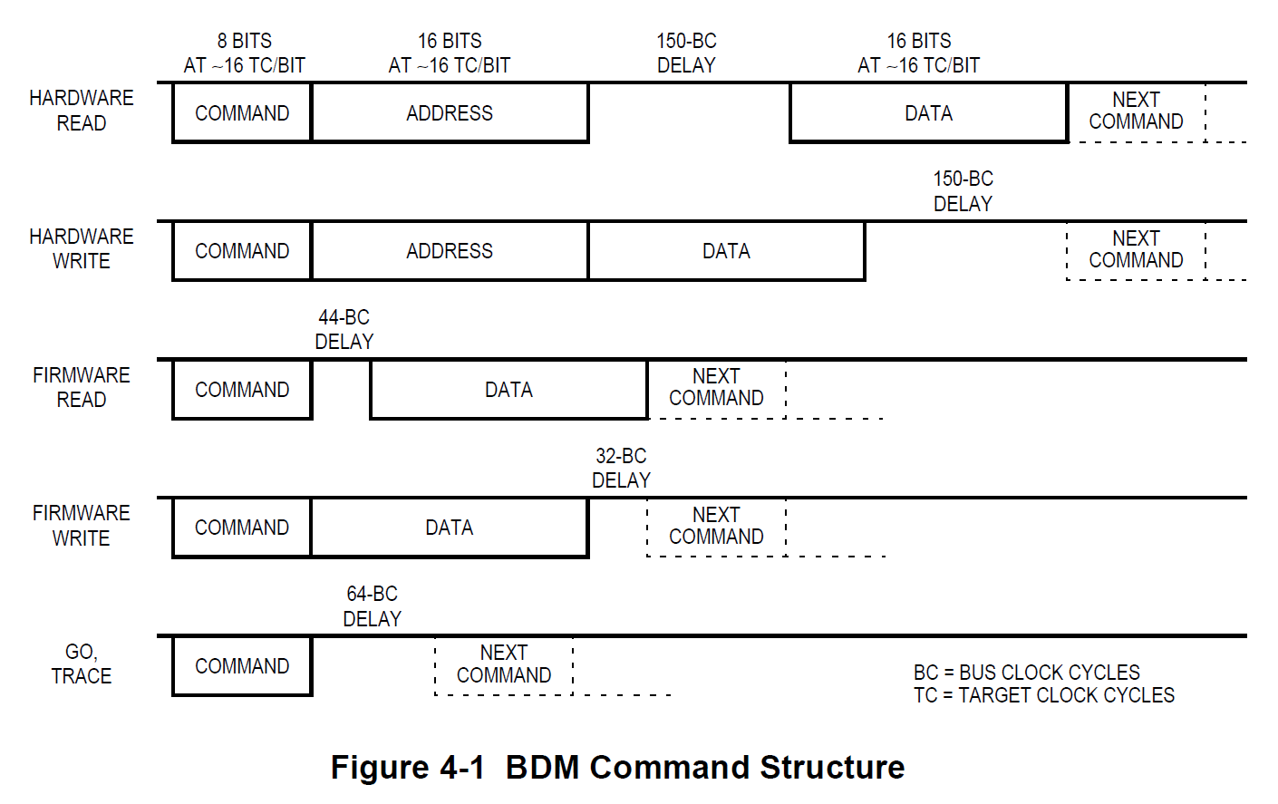
Figure 4-1 represents the BDM command structure. The command blocks illustrate a series of eight bit
times starting with a falling edge. The bar across the top of the blocks indicates that the BKGD line idles
in the high state. The time for an 8-bit command is 8 ´ 16 target clock cycles.(1)
4.6 BDM Serial Interface
The BDM communicates with external devices serially via the BKGD pin.
During reset, this pin is a mode select input which selects between normal and special modes of operation.
After reset, this pin becomes the dedicated serial interface pin for the BDM.
The BDM serial interface is timed using the clock selected by the CLKSW bit in the status register see 3.1 BDM Status Register.
This clock will be referred to as the target clock in the following explanation.
The BDM serial interface uses a clocking scheme in which the external host
generates a falling edge on the BKGD pin to indicate the start of each bit time.
This falling edge is sent for every bit whether data is transmitted or received.
Data is transferred most significant bit (MSB) first at 16 target clock cycles per bit.
The interface times out if 512 clock cycles occur between falling edges from the host.
The BKGD pin is a pseudo open-drain pin and has an weak on-chip active pull-up that is enabled at all times.
It is assumed that there is an external pull-up and that drivers connected to BKGD do not typically drive the high level.
Since R-C rise time could be unacceptably long, the target system and host provide
NOTES:
1. Target clock cycles are cycles measured using the target MCU’s serial clock rate.
See 4.6 BDM Serial Interface and 3.1 BDM Status Register for information on how serial clock rate is selected.
brief driven-high (speedup) pulses to drive BKGD to a logic 1.
The source of this speedup pulse is the host for transmit cases and the target for receive cases.
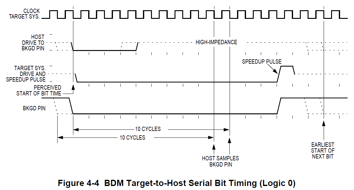
The timing for host-to-target is shown in Figure 4-2 and that of target-to-host in Figure 4-3 and Figure 4-4.
All four cases begin when the host drives the BKGD pin low to generate a falling edge.
Since the host and target are operating from separate clocks, it can take the target system up to one full clock cycle to recognize this edge.
The target measures delays from this perceived start of the bit time
while the host measures delays from the point it actually drove BKGD low to start the bit up to one target clock cycle earlier.
Synchronization between the host and target is established in this manner at the start of every bit time.
Figure 4-2 shows an external host transmitting a logic 1 and transmitting a logic 0 to the BKGD pin of a target system.
The host is asynchronous to the target, so there is up to a one clock-cycle delay from the host-generated falling edge to
where the target recognizes this edge as the beginning of the bit time.
Ten target clock cycles later, the target senses the bit level on the BKGD pin.
Internal glitch detect logic requires the pin be driven high no later that eight target clock cycles after the falling edge for a logic 1 transmission.
Since the host drives the high speedup pulses in these two cases, the rising edges look like digitally driven signals.

The receive cases are more complicated.
Figure 4-3 shows the host receiving a logic 1 from the target system.
Since the host is asynchronous to the target, there is up to one clock-cycle delay
from the host-generated falling edge on BKGD to the perceived start of the bit time in the target.
The host holds the BKGD pin low long enough for the target to recognize it (at least two target clock cycles).
The host must release the low drive
before the target drives a brief high speedup pulse seven target clock cycles after the perceived start of the bit time.
The host should sample the bit level about 10 target clock cycles after it started the bit time.
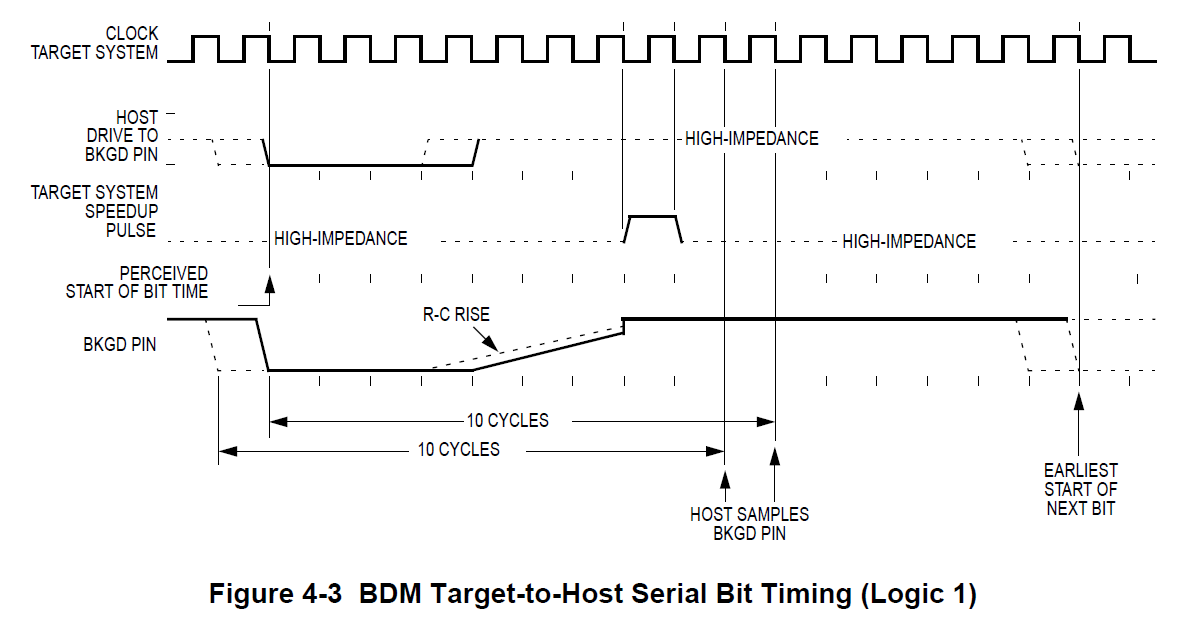
Figure 4-4 shows the host receiving a logic 0 from the target.
Since the host is asynchronous to the target, there is up to a one clock-cycle delay
from the host-generated falling edge on BKGD to the start of the bit time as perceived by the target.
The host initiates the bit time but the target finishes it.
Since the target wants the host to receive a logic 0, it drives the BKGD pin low for 13 target clock cycles
then briefly drives it high to speed up the rising edge.
The host samples the bit level about 10 target clock cycles after starting the bit time.
4.7 Serial Interface Hardware Handshake Protocol
BDM commands that require CPU execution are ultimately treated at the MCU bus rate.
Since the BDM clock source can be asynchronously related to the bus frequency,
when CLKSW = 0, it is very helpful to provide a handshake protocol in which the host could determine when an issued command is executed by the CPU.
The alternative is to always wait the amount of time equal to the appropriate number of cycles at the slowest possible rate the clock could be running.
This sub-section will describe the hardware handshake protocol.
The hardware handshake protocol signals to the host controller when an issued command was successfully executed by the target.
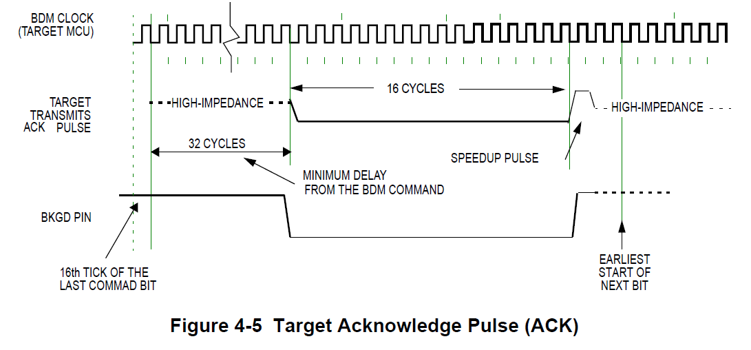
This protocol is implemented by a 16 serial clock cycle low pulse followed by a brief speedup pulse in the BKGD pin.
This pulse is generated by the target MCU when a command, issued by the host, has been successfully executed (see Figure 4-5).
This pulse is referred to as the ACK pulse.
After the ACK pulse has finished:
the host can start the bit retrieval if the last issued command was a read command,
or start a new command if the last command was a write command or
a control command (BACKGROUND, GO, GO_UNTIL or TRACE1).
The ACK pulse is not issued earlier than 32 serial clock cycles after the BDM command was issued.
The end of the BDM command is assumed to be the 16th tick of the last bit.
This minimum delay assures enough time for the host to perceive the ACK pulse.
Note also that, there is no upper limit for the delay between the command and the related ACK pulse,
since the command execution depends upon the CPU bus frequency,
which in some cases could be very slow compared to the serial communication rate.
This protocol allows a great flexibility for the POD designers,
since it does not rely on any accurate time measurement or short response time to any event in the serial communication.
NOTE:
If the ACK pulse was issued by the target, the host assumes the previous command was executed.
If the CPU enters WAIT or STOP prior to executing a hardware command, the ACK pulse will not be issued
meaning that the BDM command was not executed.
After entering wait or stop mode, the BDM command is no longer pending.
Figure 4-6 shows the ACK handshake protocol in a command level timing diagram.
The READ_BYTE instruction is used as an example.
First, the 8-bit instruction opcode is sent by the host, followed by the address of the memory location to be read.
The target BDM decodes the instruction.
A bus cycle is grabbed (free or stolen) by the BDM and it executes the READ_BYTE operation.
Having retrieved the data, the BDM issues an ACK pulse to the host controller,
indicating that the addressed byte is ready to be retrieved.
After detecting the ACK pulse, the host initiates the byte retrieval process.
Note that data is sent in the form of a word and the host needs to determine
which is the appropriate byte based on whether the address was odd or even.
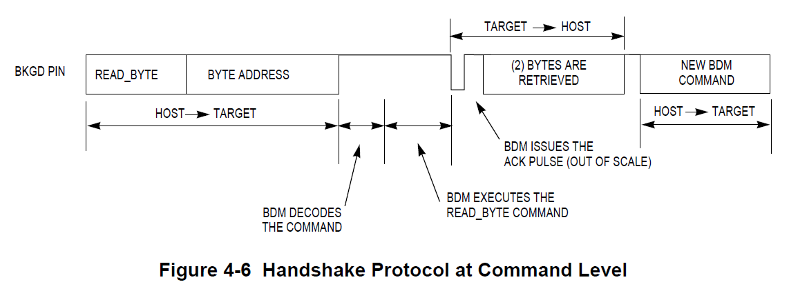
Differently from the normal bit transfer (where the host initiates the transmission),
the serial interface ACK handshake pulse is initiated by the target MCU by issuing a negedge in the BKGD pin.
The hardware handshake protocol in Figure 4-5 specifies the timing when the BKGD pin is being driven,
so the host should follow this timing constraint in order to avoid the risk of an electrical conflict in the BKGD pin.
NOTE:
The only place the BKGD pin can have an electrical conflict is
when one side is driving low and the other side is issuing a speedup pulse (high).
Other “highs” are pulled rather than driven.
However, at low rates the time of the speedup pulse can become lengthy and so the potential conflict time becomes longer as well.
The ACK handshake protocol does not support nested ACK pulses.
If a BDM command is not acknowledge by an ACK pulse, the host needs to abort the pending command first
in order to be able to issue a new BDM command.
When the CPU enters WAIT or STOP while the host issues a command that requires CPU execution (e.g., WRITE_BYTE),
the target discards the incoming command due to the WAIT or STOP being detected.
Therefore, the command is not acknowledged by the target, which means that the ACK pulse will not be issued in this case.
After a certain time the host should decide to abort the ACK sequence in order to be free to issue a new command.
Therefore, the protocol should provide a mechanism in which a command, and therefore a pending ACK, could be aborted.
NOTE:
Differently from a regular BDM command, the ACK pulse does not provide a time out.
This means that in the case of a WAIT or STOP instruction being executed, the ACK would be prevented from being issued.
If not aborted, the ACK would remain pending indefinitely.
See the handshake abort procedure described in 4.8 Hardware Handshake Abort Procedure.
4.8 Hardware Handshake Abort Procedure
The abort procedure is based on the SYNC command.
In order to abort a command, which had not issued the corresponding ACK pulse,
the host controller should generate a low pulse in the BKGD pin by driving it low for at least 128 serial clock cycles
and then driving it high for one serial clock cycle, providing a speedup pulse.
By detecting this long low pulse in the BKGD pin, the target executes the SYNC protocol, see 4.9 SYNC—Request Timed Reference Pulse,
and assumes that the pending command and therefore the related ACK pulse, are being aborted.
Therefore, after the SYNC protocol has been completed the host is free to issue new BDM commands.
Although it is not recommended, the host could abort a pending BDM command
by issuing a low pulse in the BKGD pin shorter than 128 serial clock cycles,
which will not be interpreted as the SYNC command.
The ACK is actually aborted when a negedge is perceived by the target in the BKGD pin.
The short abort pulse should have at least 4 clock cycles keeping the BKGD pin low,
in order to allow the negedge to be detected by the target.
In this case, the target will not execute the SYNC protocol but the pending command will be aborted along with the ACK pulse.
The potential problem with this abort procedure is when there is a conflict between the ACK pulse and the short abort pulse.
In this case, the target may not perceive the abort pulse.
The worst case is when the pending command is a read command (i.e., READ_BYTE).
If the abort pulse is not perceived by the target the host will attempt to send a new command after the abort pulse was issued,
while the target expects the host to retrieve the accessed memory byte.
In this case, host and target will run out of synchronism.
However, if the command to be aborted is not a read command the short abort pulse could be used.
After a command is aborted the target assumes the next negedge, after the abort pulse, is the first bit of a new BDM command.
NOTE:
The details about the short abort pulse are being provided only as a reference for the reader to better understand the BDM internal behavior.
It is not recommended that this procedure be used in a real application.
Since the host knows the target serial clock frequency,
the SYNC command (used to abort a command) does not need to consider the lower possible target frequency.
In this case, the host could issue a SYNC very close to the 128 serial clock cycles length.
Providing a small overhead on the pulse length in order to assure the SYNC pulse will not be misinterpreted by the target.
See 4.9 SYNC — Request Timed Reference Pulse.
Figure 4-7 shows a SYNC command being issued after a READ_BYTE, which aborts the READ_BYTE command.
Note that, after the command is aborted a new command could be issued by the host computer.
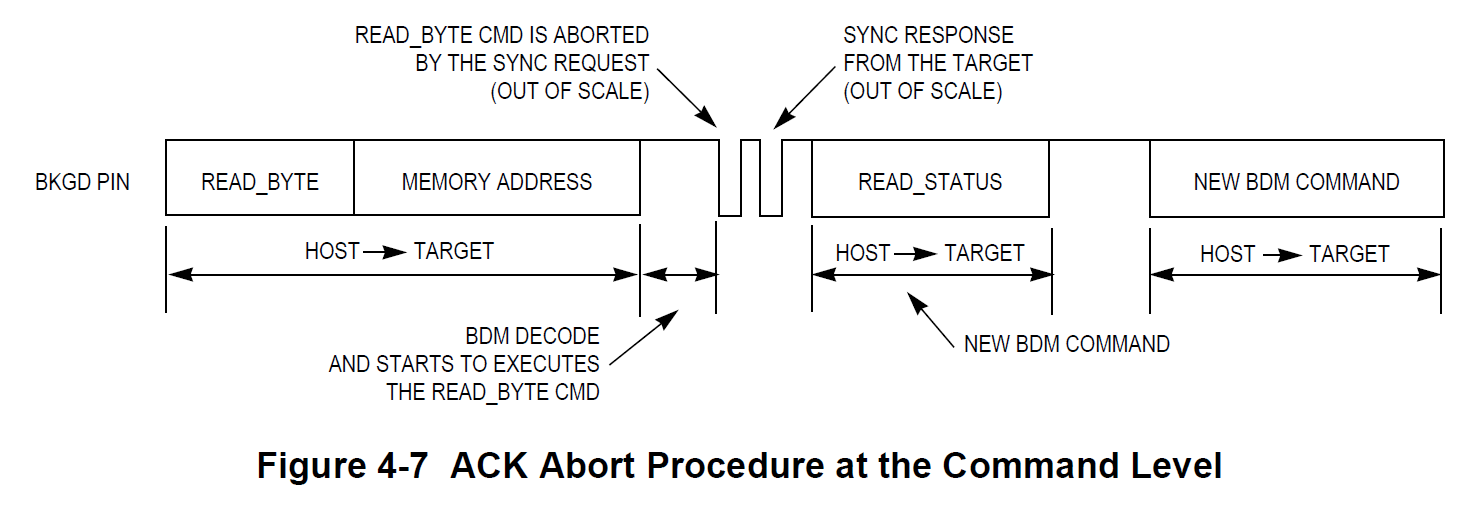
NOTE: Figure 4-7 does not represent the signals in a true timing scale
Figure 4-8 shows a conflict between the ACK pulse and the SYNC request pulse.
This conflict could occur if a POD device is connected to the target BKGD pin and the target is already in debug active mode.
Consider that the target CPU is executing a pending BDM command at the exact moment the POD is being connected to the BKGD pin.
In this case, an ACK pulse is issued along with the SYNC command.
In this case, there is an electrical conflict between the ACK speedup pulse and the SYNC pulse.
Since this is not a probable situation, the protocol does not prevent this conflict from happening.
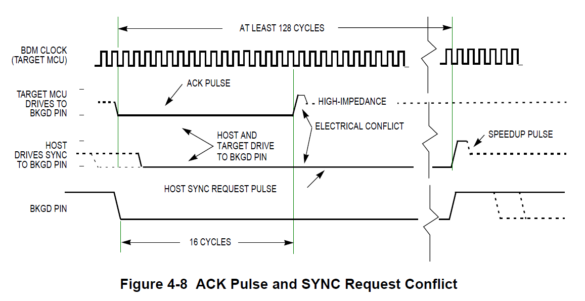
NOTE: This information is being provided so that the MCU integrator will be aware that such a conflict could eventually occur.
The hardware handshake protocol is enabled by the ACK_ENABLE and disabled by the ACK_DISABLE BDM commands.
This provides backwards compatibility with the existing POD devices which are not able to execute the hardware handshake protocol.
It also allows for new POD devices, that support the hardware handshake protocol,
to freely communicate with the target device. If desired, without the need for waiting for the ACK pulse.
The commands are described as follows:
• ACK_ENABLE—enables the hardware handshake protocol.
The target will issue the ACK pulse when a CPU command is executed by the CPU.
The ACK_ENABLE command itself also has the ACK pulse as a response.
• ACK_DISABLE— disables the ACK pulse protocol.
In this case, the host needs to use the worst case delay time at the appropriate places in the protocol.
The default state of the BDM after reset is hardware handshake protocol disabled.
All the read commands will ACK (if enabled) when the data bus cycle has completed
and the data is then ready for reading out by the BKGD serial pin.
All the write commands will ACK (if enabled) after the data has been received
by the BDM through the BKGD serial pin and when the data bus cycle is complete.
See 4.3 BDM Hardware Commands and 4.4 Standard BDM Firmware Commands for more information on the BDM commands.
The ACK_ENABLE sends an ACK pulse when the command has been completed.
This feature could be used by the host to evaluate if the target supports the hardware handshake protocol.
If an ACK pulse is issued in response to this command, the host knows that the target supports the hardware handshake protocol.
If the target does not support the hardware handshake protocol the ACK pulse is not issued.
In this case, the ACK_ENABLE command is ignored by the target since it is not recognized as a valid command.
The BACKGROUND command will issue an ACK pulse when the CPU changes from normal to background mode.
The ACK pulse related to this command could be aborted using the SYNC command.
The GO command will issue an ACK pulse when the CPU exits from background mode.
The ACK pulse related to this command could be aborted using the SYNC command.
The GO_UNTIL command is equivalent to a GO command with exception that the ACK pulse,
in this case, is issued when the CPU enters into background mode.
This command is an alternative to the GO command and should be used when the host wants to trace
if a breakpoint match occurs and causes the CPU to enter active background mode.
Note that the ACK is issued whenever the CPU enters BDM,
which could be caused by a Breakpoint match or by a BGND instruction being executed.
The ACK pulse related to this command could be aborted using the SYNC command.
The TRACE1 command has the related ACK pulse issued when the CPU enters background active mode
after one instruction of the application program is executed.
The ACK pulse related to this command could be aborted using the SYNC command.
The TAGGO command will not issue an ACK pulse since this would interfere with the tagging function shared on the same pin.
4.9 SYNC — Request Timed Reference Pulse
The SYNC command is unlike other BDM commands
because the host does not necessarily know the correct communication speed
to use for BDM communications until after it has analyzed the response to the SYNC command.
To issue a SYNC command, the host should perform the following steps:
1. Drive the BKGD pin low for at least 128 cycles at the lowest possible BDM serial communication frequency
(the lowest serial communication frequency is determined by the crystal oscillator or the clock chosen by CLKSW.)
2. Drive BKGD high for a brief speedup pulse to get a fast rise time (this speedup pulse is typically one cycle of the host clock.)
3. Remove all drive to the BKGD pin so it reverts to high impedance.
4. Listen to the BKGD pin for the sync response pulse.
Upon detecting the SYNC request from the host, the target performs the following steps:
1. Discards any incomplete command received or bit retrieved.
2. Waits for BKGD to return to a logic one.
3. Delays 16 cycles to allow the host to stop driving the high speedup pulse.
4. Drives BKGD low for 128 cycles at the current BDM serial communication frequency.
5. Drives a one-cycle high speedup pulse to force a fast rise time on BKGD.
6. Removes all drive to the BKGD pin so it reverts to high impedance.
The host measures the low time of this 128 cycle SYNC response pulse and determines the correct speed for subsequent BDM communications.
Typically, the host can determine the correct communication speed within a few percent of the actual target speed
and the communication protocol can easily tolerate speed errors of several percent.
As soon as the SYNC request is detected by the target, any partially received command or bit retrieved is discarded.
This is referred to as a soft-reset, equivalent to a time-out in the serial communication.
After the SYNC response, the target will consider the next negedge (issued by the host)
as the start of a new BDM command or the start of new SYNC request.
Another use of the SYNC command pulse is to abort a pending ACK pulse.
The behavior is exactly the same as in a regular SYNC command.
Note that one of the possible causes for a command to not be acknowledged by the target is a host-target synchronization problem.
In this case, the command may not have been understood by the target and so an ACK response pulse will not be issued.
/* OSBDM-JM60 Target Interface Software Package
 * Copyright (C) 2009  Freescale
 *
 * This software package is free software; you can redistribute it and/or
 * modify it under the terms of the GNU Lesser General Public
 * License as published by the Free Software Foundation; either
 * version 2 of the License, or (at your option) any later version.
 *
 * This software is distributed in the hope that it will be useful,
 * but WITHOUT ANY WARRANTY; without even the implied warranty of
 * MERCHANTABILITY or FITNESS FOR A PARTICULAR PURPOSE.  See the GNU
 * Lesser General Public License for more details.
 *
 * You should have received a copy of the GNU Lesser General Public
 * License along with this software; if not, write to the Free Software
 * Foundation, Inc., 59 Temple Place, Suite 330, Boston, MA  02111-1307  USA
 */

/*****************************************************************************\
*
 * Author:   Axiom Manufacturing
 *
 * File:   bdm_bgnd_driver.h
 *
 * Purpose:  Header file for bdm_bgnd_driver.c file
 *
 \*****************************************************************************/

#ifndef _BDM_BGND_DRIVER_H_
#define _BDM_BGND_DRIVER_H_

// BDM BGND driver API functions

void BgndInit( void );

void BgndProgPower( byte enable );

void BgndProgEnable( byte enable );

UINT16 BgndGetClock( void );

void BgndSetClock( UINT16 interval );

UINT16 BgndSync( void );

byte BgndReset( byte mode );

byte BgndAckSupported( void );

byte BgndResetDetect( void );

byte BgndClockState( void );

void BgndUnsecure( void );

byte BgndTxRx( Pbyte pTxData, Pbyte pRxData, byte TxCount, byte RxCount );

#endif // _BDM_BGND_DRIVER_H_
// --------------------------------- EOF -------------------------------------
/* OSBDM-JM60 Target Interface Software Package
 * Copyright (C) 2009  Freescale
 *
 * This software package is free software; you can redistribute it and/or
 * modify it under the terms of the GNU Lesser General Public
 * License as published by the Free Software Foundation; either
 * version 2 of the License, or (at your option) any later version.
 *
 * This software is distributed in the hope that it will be useful,
 * but WITHOUT ANY WARRANTY; without even the implied warranty of
 * MERCHANTABILITY or FITNESS FOR A PARTICULAR PURPOSE.  See the GNU
 * Lesser General Public License for more details.
 *
 * You should have received a copy of the GNU Lesser General Public
 * License along with this software; if not, write to the Free Software
 * Foundation, Inc., 59 Temple Place, Suite 330, Boston, MA  02111-1307  USA
 */

/*****************************************************************************\
*
 * Author:   Axiom Manufacturing
 *
 * File:   bdm_bgnd_driver.c
 *
 * Purpose:  BDM BGND driver file
 *       Does not support the hardware handshake protocol
 *
 \*****************************************************************************/

#include "derivative.h"     // Include peripheral declarations
#include "typedef.h"      // Type definitions
#include "MCU.h"        // MCU header
#include "timer.h"        // Timer functions
#include "bdm_bgnd_driver.h"    // Driver header
#include "target.h"       // Target specific definitions

// ---------------------------------------------------------------------------
// Internal definitions
// ---------------------------------------------------------------------------

// BgndReset() support definitions

#define TRESET_OUT  PTCD_PTCD4
#define TBGND_IN    PTFD_PTFD1
#define TBGND_OUT   PTFD_PTFD4
#define TBGND_EN    PTFD_PTFD5

#define TRESET_OUT_DD PTCDD_PTCDD4
#define TBGND_IN_DD   PTFDD_PTFDD1
#define TBGND_OUT_DD  PTFDD_PTFDD4
#define TBGND_EN_DD   PTFDD_PTFDD5

// Internal prototypes
void BgndDetect( void );
void BgndTimerCompute( void );

// ---------------------------------------------------------------------------
// Internal variables
// ---------------------------------------------------------------------------
static byte TimersInited = FALSE;  // 1 when timers are usable by the driver
static byte ClockSet = FALSE;      // TRUE when rate set manually, no sync permitted
static UINT16 syncTime;            // Sync interval in 24 MHz timer ticks
static UINT16 interval;            // The returned interval, assuming timeout

#pragma DATA_SEG __SHORT_SEG _DATA_ZEROPAGE

UINT16 bit1Time;       // Timer ticks representing the 1 bit pulse length
UINT16 bitThreshold;   // Timer ticks representing the 0/1 threshold
UINT16 bit0Time;       // Timer ticks representing the 0 bit pulse length
UINT16 bitTime;        // Timer ticks representing the 16 target clocks interval
Pbyte pBytes;          // Pointer into the TX/RX buffers
UINT8 bitsLeft;        // Number of remaining bits to be sent/received
UINT8 bytesLeft;       // Number of remaining bytes to be sent/received
UINT16 bitSTime;       //

#pragma DATA_SEG DEFAULT

// ---------------------------------------------------------------------------
// Initialize the driver
// ---------------------------------------------------------------------------
void BgndInit( void )
{
  TimersInited = FALSE;     // Ensure timers will be programmed before use
  ClockSet = FALSE;         // Show the BDM clock is not manually configured
  BgndProgPower( 0 );       // Ensure programming power supply is off
  BgndProgEnable( 0 );      // Ensure programming voltage is not applied
}

// ---------------------------------------------------------------------------
// Enable/Disable the 12 volt programming power (only used for 9RS08)
// ---------------------------------------------------------------------------
void BgndProgPower( byte enable )
{
  PTFD_PTFD0 = 0;     // Disable the programming voltage to the chip
#if 1
  PTFDD_PTFDD0 = 1;   // Make the enable pin an output
#endif

  TPM1C2SC = 0;       // Disable the timer channel (release the pin)
  PTCD_PTCD5 = ( ( enable ) ? ( 1 ) : ( 0 ) );

#if 1
  PTCDD_PTCDD5 = 1;   // Make the programming power pin an output
#endif

  wait_ms( 2 );       // Time for power to settle
}

// ---------------------------------------------------------------------------
// Enable/Disable the 12 volt programming power to the chip (restartable)
// ---------------------------------------------------------------------------
void BgndProgEnable( byte enable )
{
  PTFD_PTFD0 = 0;   // Disable the programming voltage to the chip
  RTCSC = 0x80;     // Disable the timer (dismisses the flag)

  if ( enable )
  {
    PTFD_PTFD0 = 1; // Enable the programming voltage to the chip
    RTCMOD = 5;     // Turn on the timer for 6 mSec
    RTCSC = 0x33;   // RTCLKS = 01, RTIE = 1, RTCPS = 3
  }
}

// ---------------------------------------------------------------------------
// VPP timer ISR, to ensure programming power disable
// ---------------------------------------------------------------------------
void interrupt
VPP_ISR( void )
{
  PTFD_PTFD0 = 0;          // Disable the programming voltage to the chip
  RTCSC = 0x80;            // Disable the timer (dismisses the interrupt)
  if ( FP_Stat == FP_RUNNING )
  {                        // if we're programming flash
    FP_Stat = FP_TIMEOUT;  // set status - timeout waiting for flash algo to finish
  }
}

// ---------------------------------------------------------------------------
// Get the current sync interval (in 60 MHz ticks)
// ---------------------------------------------------------------------------
// Returns the detected/configured sync interval
UINT16 BgndGetClock( void )   // in 60 MHz ticks
{
  UINT32 temp = syncTime;

  if ( syncTime == 0 )
    return ( 0 );                                   // Not set yet, report don't know
  return ( UINT16 )( ( ( temp * 5 ) + 1 ) >> 1 );   // Set already, convert it
}

/* ---------------------------------------------------------------------------
 Set the interface clock externally, using the interval (in 60 MHz ticks)
 This can be called in place of BgndSync() to configure for a specified rate
 Example - to set oscillator at 4Mhz:
 (1 / 4,000,000) * 256 / (1/60,000,000) = freq to set in 60Mhz ticks
 (1 / 4,000,000) * 15360000000 = 3840 (0xF00, which is the value sent from the PC)
 3840 / 2.5 = 1536 (Synctime)  or  (3840 * 2) / 5
 NOTE: lowest frequency this math will support is 500Khz
 */

// ---------------------------------------------------------------------------
void BgndSetClock( UINT16 request ) // The duration of the detected interval, in 60 MHz ticks
{
  UINT32 temp = request;
  if ( request != 0 )
  {
    ClockSet = TRUE;
    syncTime = ( UINT16 )( ( temp * 2 ) / 5 );
  }
  else /* request == 0 */
  {
    ClockSet = FALSE;
    syncTime = BgndSync( );
  }
  BgndTimerCompute( );
}

// ---------------------------------------------------------------------------
// Sync to the target interface bit clock by detecting the rate
// Also configures the driver parameters for the detected target bit clock
// ---------------------------------------------------------------------------
// Returns the detected sync interval, or 0  for timeout
UINT16 BgndSync( void )
{
  if ( ClockSet == FALSE )
  {
    BgndDetect( );             // Try to determine the target clock
    BgndTimerCompute( );
  }
  return ( BgndGetClock( ) );  // Return the current value
}

// ---------------------------------------------------------------------------
//  Get the target bit clock timing information
// ---------------------------------------------------------------------------
void BgndDetect( void )   // Returns 0 if no target, or detection timeout
{
  interval = 0;           // clear interval timer
  TPM1SC = 0;             // Clear/reset all timers
  TPM2SC = 0;
  TPM1C3SC = 0;
  TPM2C0SC = 0;
  TPM2C1SC = 0;

  TBGND_OUT = 1;         // Set TBGND_OUT active high
  TBGND_OUT_DD = 1;      // Signal is output

  TBGND_EN = 1;          // Set TBGND_EN direction A to B
  TBGND_EN_DD = 1;       // Signal is output, dir set A to B

  TPM1MOD =              // Set timer modulus
  TPM2MOD = 0x4000;      // Set timer modulus
  TPM1CNTH = 0;          // Reset the counters so they will restart
  TPM2CNTH = 0;          // into the modulus range, delta of 5 ticks

  TPM2C0V = 0;           // Hold TBGND_OUT high when not pulsed
  TPM2C1V = 0xFFFF;      // Hold TBGND_EN  low  when not pulsed

  TPM2C0SC = 0x24;       // Enable the TBGND_OUT timer channel, pulses low
  TPM2C1SC = 0x28;       // Enable the TBGND_EN  timer channel, pulses high
  TPM1C3SC = 0x0c;       // Capture both edges

  TPM1SC = 0x08;         // Start timer 1
  TPM2SC = 0x08;         // Start timer 2

  TPM2C0V = 0x20D0;      // Set TBGND_OUT pulse low  width
  TPM2C1V = 0x20D2;      // Set TBGND_EN  pulse high width

  if ( TPM2SC_TOF )
    TPM2SC_TOF = 0;

  while ( !TPM2SC_TOF ) // Wait for rollover on timer 2 (start of sync pulse)
    ;
  TPM2SC_TOF = 0;

  TPM2C0V = 0;          // No second pulse on T2C0
  TPM2C1V = 0xFFFF;     // No second pulse on T2C1

  if ( TPM2C0SC_CH0F )
    TPM2C0SC_CH0F = 0;

  while ( !TPM2C0SC_CH0F )  // Wait for end of sync pulse on TBGND_OUT
    ;

  if ( TPM1C3SC_CH3F )
  {
    TPM1C3SC = 0x0c;        // Capture both edges
  }
  TPM2C0SC = 0;             // (5) Reset the falling transition capture channel
  while ( !TPM2SC_TOF )
  {    // Wait for rollover on timer 2 (end of measurement)
    if ( TPM1C3SC_CH3F )
    {
      interval = TPM1C3V;
      TPM1C3SC = 0x0c;      // Capture both edges
      break;
    }
  }
  while ( !TPM2SC_TOF )
  {    // Wait for rollover on timer 2 (end of measurement)
    ;
  }
  if ( TPM1C3SC_CH3F )
  {
    syncTime = TPM1C3V;
  }

  TPM2C0SC = 0;        // Clear/reset all timers
  TPM2C1SC = 0;
  TPM2SC = 0;
  TPM1C3SC = 0;
  TPM1SC = 0;
  TBGND_EN = 0;        // Set the bus transceiver to B to A (Hi-Z)

  TimersInited = FALSE;

  if ( syncTime != 0 )
  {
    syncTime = ( syncTime - interval );
  }
}

// ---------------------------------------------------------------------------
// Assert hardware reset to target device
// ---------------------------------------------------------------------------
// Returns 0 for success; can't fail
byte BgndReset( byte mode )
// 0 = Hard reset to BDM mode;
// 1 = Hard reset to Running Mode;
// 2 = Voltage reset to BDM mode
{
  TPM1SC = 0;      // Clear/reset all timers
  TPM2SC = 0;
  TPM1C3SC = 0;
  TPM2C0SC = 0;
  TPM2C1SC = 0;

  TBGND_EN = 0;      // Prepare to set BGND pin hi-z, (B to A)
  TBGND_EN_DD = 1;      // Set pin as out to transceiver

  TBGND_OUT = 0;      // Prepare to set TBGND_OUT signal to low
  TBGND_OUT_DD = 1;      // Set pin as out low to transceiver

  TRESET_OUT = 0;      // Prepare to assert reset hi-Z to target
  TRESET_OUT_DD = 1;      // Set pin as out to target (hi-Z)

  TPM2SC = 0;      // Clear timer 2 TOF, set divider to 1
  TPM2C0SC = 0;      // Set timer2 channel 0 pin as GPIO
  TPM2MOD = 0x0800; // Load timer2 count (85.3us pulse width) how long reset is active

  if ( mode == 2 )        // If voltage reset mode
    VTRG_EN = 0;      // remove power from the target
  else
    TRESET_OUT = 1;     // Assert reset active low to target

  if ( mode == 0 || mode == 2 ) // If BDM active mode:
    TBGND_EN = 1;      // Swap the transceiver to assert BGND low to target
  // Otherwise, it floats high to target
  TPM2SC = 0x08;   // Start counting at bus rate clk
  while ( !TPM2SC_TOF )
    // Wait for timer2 TOF to set
    ;

  TPM2SC_TOF = 0;      // Clear TOF bit

  wait_ms( 25 );        // Allow time for power off

//  if delay above is moved to only voltage reset mode,
//  then this delay is required by the DEMO9S12XSFAME, no sure why
//  wait_ms(8);

  // If voltage reset mode
  if ( mode == 2 )
  {
    VTRG_EN = 1;      // restore power to the target
  }
  else
    TRESET_OUT = 0;     // De-assert reset out (back to hi-Z)

  if ( mode == 0 || mode == 2 ) // If BDM active mode:
  {           // Hold BGND low as target exits reset
    TPM2SC = 0;      // Disable timer
    TPM2MOD = 0x0200;  // Load timer count (21.2us /TBGND hold time after reset)
    TPM2SC = 0x08;   // Start counting at bus rate clk
    while ( !TPM2SC_TOF )
      // Wait for timer2 TOF to set
      ;
    TBGND_OUT = 1;      // Raise the TBGND_OUT signal to high
    TBGND_EN = 0;      // Swap the transceiver to float BGND back to hi-z
  }

  TPM2SC = 0;      // Disable timer 2
  TBGND_EN = 0;      // Set the bus transceiver to B to A (Hi-Z)
  TimersInited = FALSE;
  wait_ms( 10 );        // Allow time to get running
  return ( 0 );         // Return unconditional success
}

// ---------------------------------------------------------------------------
// Internal definitions for the BGND W/R driver
// ---------------------------------------------------------------------------
#define  TPMINIT   0x08 // Enabled, bus clock div 1   used by the W/R driver
#define  TPM13INIT 0x04 // Enabled, input capture mode
#define  TPM20INIT 0x24 // Enabled, BGNDOUT pulses low
#define  TPM21INIT 0x28 // Enabled, A -> B

// Target bit clock support definitions for 24 MHz target clock
UINT16 const bit1Time24 = 4;    // Timer ticks representing the 1 bit pulse length @24MHz
UINT16 const bitThresh24 = 10;  // Timer ticks representing the threshold time
UINT16 const bit0Time24 = 13;   // Timer ticks representing the 0 bit pulse length @24MHz
UINT16 const bitTime24 = 50;    // Timer ticks representing the minimum bit time
//                              // (required by the driver code)

void BgndTimerCompute_C( void )
{
  //  if (syncTime != 0)
  if ( syncTime >= 0x83 )     // 24Mhz is as fast as we can run
  {
    // Bit1 time is 4/16 of a bit time, rounded
    bit1Time = ( syncTime + 16 ) / 32;
    // Bit threshold is 10/16 of a bit time, rounded
    bitThreshold = ( ( ( ( syncTime + 8 ) / 16 ) * 10 ) + 4 ) / 8;
    // Bit0 time is 13/16 of a bit time, rounded
    bit0Time = ( ( ( ( syncTime + 8 ) / 16 ) * 13 ) + 4 ) / 8;
    // Bit time is rounded, and must be slightly > target bit time
    bitTime = ( ( syncTime + 4 ) / 8 ) + 1;

    if ( bitTime < bitTime24 )
      bitTime = bitTime24;    // Minimum value needed by firmware

    // In this computation, the +5 is because TPM1 is 5 ticks higher than TPM2
    // In this computation, the +1 is because TPM1 capture is low by one
    bitThreshold += 5 + 1;
  }

  else // Default initialization; for 24 MHz target bit clock
  {
    bit1Time = bit1Time24;
    // bitThreshold = bitThresh24;
    bitThreshold = 14;
    bit0Time = bit0Time24;
    bitTime = bitTime24;
  }
}

void BgndTimerCompute_ASM(void)
{
#asm
// Divide by 8 with round up
Div8r:
  ldhx syncTime
  pshh
  txa
  pulx

  lsrx  // divide by 8
  rora
  lsrx
  rora
  lsrx
  rora
  adc #0
  bcc bgndTC01  // round up
  aix #1
bgndTC01:
  pshx   // save bitTime
  psha

  lsrx
  rora

  adc #0
  bcc bgndTC02  // round up
  aix #1
bgndTC02:

  pshx  // save 8 cycle time
  psha
  lsrx
  rora

  adc #0
  bcc bgndTC03  // round up
  aix #1
bgndTC03:

  pshx  // save 4 cycle time
  psha

  lsrx  // compute 2 cycle time
  rora

  adc #0
  bcc bgndTC04  // round up
  aix #1
bgndTC04:

  pshx  // save 2 cycle time
  psha

  pulx  // pull 2 cycle time
  pulh

  sthx bitThreshold

  pulx  // pull 4 cycle time
  pulh
  sthx bit1Time

  pulx  // pull 8 cycle time
  pulh
  sthx bit0Time

  pulx
  pulh
  sthx bitTime
#endasm
}

// ---------------------------------------------------------------------------
// Sync to the target interface bit clock using the syncTime value
// ---------------------------------------------------------------------------
void BgndTimerCompute( void )
{
  BgndTimerCompute_ASM( );

  bitThreshold += bit0Time;
  bit0Time += bit1Time;
  //  bitSTime = bit0Time + 10;

  if ( bitTime < bitTime24 )
  {
    bitTime = bitTime24;    // Minimum value needed by firmware
  }
  bitSTime = bitTime - 10;

  //  bitThreshold += 5 + 2;  // this worked with gold version
  bitThreshold += 5 + 5;    // 8 to 13 may be best for the new version

  TimersInited = FALSE;
}

// ---------------------------------------------------------------------------
// Initialize the driver timers
// ---------------------------------------------------------------------------
void BgndInitTimers( void )
{
  TPM1SC = 0;      // Stop all the timers
  TPM2SC = 0;
  TPM1C3SC = 0;
  TPM2C0SC = 0;
  TPM2C1SC = 0;

  TPM1MOD = 1;      // Set modulus low for fast register update
  TPM2MOD = 1;

  TPM1CNTH = 0;      // Reset the counters so they will restart
  TPM2CNTH = 0;      // into the modulus range

  // Resetting the timers as follows results in TPM1 being 5 counts higher
  // than TPM2, which is compensated in the computation of bitThreshold.
  // See BgndRate() for this computation.
  TPM1C3SC = TPM13INIT;  // Initialize the receive capture mode
  TPM2C0SC = TPM20INIT;  // Enable the BGND out timer channel, pulses low
  TPM2C1SC = TPM21INIT; // Set the XCVR out timer channel HIGH (Output to target)

  TPM2C0V = 0;      // Output will start after setting TPMnCmV != 0
  TPM2C1V = 0xFFFF;   // Set to hold XCVR in Output mode (hi level)

  TPM1MOD = bitTime;  // Set the real bit time periods
  TPM2MOD = bitTime;

  TPM1SC = TPMINIT;  // Start the RX timer counter (must be first)
  TPM2SC = TPMINIT;  // Start the TX timer counter (must be second)

  TPM1CNTH = 0;      // Reset the counters so they will restart
  TPM2CNTH = 0;      // into the current modulus range

  wait_ms( 1 );
  TimersInited = TRUE;
}

// ---------------------------------------------------------------------------
// Report whether the device/driver supports the ACK protocol
// ACK support:  WAIT = 0,  ACKN = 1
// ---------------------------------------------------------------------------
byte BgndAckSupported( void )
{
  return ( 0 );   // This driver does not support the ACK protocol
}

// ---------------------------------------------------------------------------
// Report any detected reset occurences
// Reset detect:  No = 0,  Yes = 1
// ---------------------------------------------------------------------------
byte BgndResetDetect( void )
{
  return t_rsti( );  // check if target is in reset
}

// ---------------------------------------------------------------------------
// Report the state of the BDM clock configuration
// Clock mode:  NO connection = 0,  SYNC = 1,  Manual set = 3
// ---------------------------------------------------------------------------
byte BgndClockState( void )
{
  return ( ( syncTime == 0 ) ? 0 : ( ClockSet ? 3 : 1 ) );
}

// ---------------------------------------------------------------------------
// Unsecure flash by erasing it and resetting the security code
// ---------------------------------------------------------------------------
void BgndUnsecure( void )   // This is implemented a different way elsewhere
{
}

// BWJ TEMPORARY CODE TO TEST THE +12V GENERATOR
void PulsePower( void )
{
  BgndProgPower( 1 );

  BgndProgEnable( 1 );
  dly_10us( 2 );
  BgndProgEnable( 0 );
  wait_ms( 1 );

  BgndProgPower( 0 );
  wait_ms( 20 );
}

void testgen( void )
{
  for ( ;; )
    PulsePower( );
}
// BWJ END OF TEMPORARY CODE TO TEST THE +12V GENERATOR

// ---------------------------------------------------------------------------
// Perform a requested write followed by read via the hardware
// ---------------------------------------------------------------------------
// Returns 0 for success, else 1 for ACK timeout
byte BgndTxRx( Pbyte pTxData, Pbyte pRxData, byte TxCount, byte RxCount )
{
  byte ccr;                     // Saved interrupt status
  byte status = 0;              // Returned status

  if ( !TimersInited )          // Ensure sure the timers are running
    BgndInitTimers( );

  // set up Reset input detect, just in case Soft reset to BGND mode...
  KBIES = 0x04;                 //  Rising edge detect
  KBIPE = 0x04;                 //  enable Port D2...
  KBISC = 0x04;                 //  set mode and clear flag...

#asm
  tpa                           // Condition codes to A
  sta ccr                       // Save old interrupt status
  sei                           // Disable interrupts

  // Perform the TxData write, if requested
  ldhx  #$FFFF                  // Ensure bus transceiver is constant Output mode (A to B)
  sthx  TPM2C1VH

  ldx TxCount                   // Init bytesLeft (in DIRECT space)
  beq txdone                    // Write not requested (never legit)

  stx bytesLeft
  ldhx  pTxData                 // Init pBytes (in DIRECT space)
wloop1:
  brclr 7, TPM2SC, wloop1       // 5, Synchronize to the bit clock
  mov #TPMINIT, TPM2SC          // 4, Reset the flag bit
  bra entertx                   // 3, Enter the main TX loop// x:h->TxData

// Send buffer loop
nexttxbyte:
  ldhx  pBytes                  // 4, Get and increment the data pointer
  aix #1                        // 2

entertx:
  sthx  pBytes                  // 4, Save the data pointer
  lda ,x                        // 3, Get the first/next byte
  ldx #8                        // 2, Set the remaining bit loop count
  stx bitsLeft                  // 3

// Send byte loop
nexttxbit:
  lsla                          // 1, Test the MSB and shift it one
  bcs use1bit                   // 3

  ldhx  bit0Time                // 4, Use the 0-bit timer value
wloop3:
  brclr 7, TPM2SC, wloop3       // 5, Await the current bit pulse end
  mov #TPMINIT, TPM2SC          // 4, Reset the flag bit
  sthx  TPM2C0VH                // 4, Set the next bit time
  dbnz  bitsLeft,  nexttxbit    // 7, Continue while 7 bits not done
  bra wbit8                     // 3, Go complete the eight bit

use1bit:
  ldhx  bit1Time                // 4, Use the 1-bit timer value
wloop4:
  brclr 7, TPM2SC, wloop4       // 5, Await the current bit pulse end
  mov #TPMINIT, TPM2SC          // 4, Reset the flag bit
  sthx  TPM2C0VH                // 4, Set the next bit time
  dbnz  bitsLeft, nexttxbit     // 7, Continue while 7 bits not done

// Await the bit 7 completion, and the start of bit 8
wbit8:
  clrh                          // 1, Set zero pulse length to hold
  clrx                          // 1, the output high for a bit time
wloop5:
  brclr 7, TPM2SC, wloop5       // 5, Await the bit 7 -8 transition
  mov #TPMINIT, TPM2SC          // 4, Reset the flag bit
  sthx  TPM2C0VH                // 4, Set the idle bit value (0), BGND output = 1
  dbnz  bytesLeft, nexttxbyte   // 7, Continue while buffer not done

txdone:

// Prepare to receive RX data input: initiate reception, if requested
  ldx RxCount                   // 3, Init bytesLeft (in DIRECT space)
  bpl BgndRx                    // 3, Go receive with valid byte count

//*** Soft Reset to BDM mode here, RxCount = 0x80 or higher....
// Force BGND low now....
  ldhx  #0xFFFF                 // 3, set the timer to do it
  sthx  TPM2C0VH                // 4, BGND low on next bit timer out

SR_BDM1:
  brclr 7, TPM2SC, SR_BDM1      // 5, Await the current bit period end

// setup timeout
  clrh                          // set timer to free running
  clrx
  stx TPM1SC                    // Timer 1 is off
  sthx  TPM1MODH                // set max timer (2.73 ms) (low timer byte)
  mov #TPMINIT, TPM1SC          // 4, Start the timer again
  stx TPM1CNTH                  // Reset timer counter to 0 for msx time

  //clra                        // set max timeout = 700 ms  (high timer byte)
  lda #0x70                     // set timeout = 300 ms  (high timer byte)

// BGND is low now, wait for Reset edge...
SR_BDM2:
  // BRSET 3, KBISC, SR_BDM2a   // finish if reset high

// check for timeout
  BRCLR 7, TPM1SC, SR_BDM2      // check timout timer (LB)
  mov #TPMINIT, TPM1SC          // 4, Reset the flag bit
  dbnza   SR_BDM2               // check timeout timer (HB)
SR_BDM2a:

  mov #TPMINIT, TPM2SC          // 4, Reset the flag bit
// already clear
// clrh                         // 1, Set zero pulse length to hold
// clrx                         // 1, the output high for a bit time
SR_BDM3:
  brclr 7, TPM2SC, SR_BDM3      // 5, Await the current bit period end
  mov #TPMINIT, TPM2SC          // 4, Reset the flag bit
  sthx  TPM2C0VH                // 4, Set the idle bit value (0), BGND output = 1

SR_BDM4:
  brclr 7, TPM2SC, SR_BDM4      // 5, Await the current bit period end
  mov #TPMINIT, TPM2SC          // 4, Reset the flag bit
  bra rxdone                    // finsihed

//............................................................
// Receive bytes here....

BgndRx:
  beq rxdone                    // 3, Read not requested// just return

  stx bytesLeft                 // 3
  ldhx  pRxData                 // 4, Init pBytes (in DIRECT space)
  sthx  pBytes                  // 4,

//............................................................
// Receive buffer loop

enterRX:
  lda #BDMRXDELAY               // 2, Load the RX extra delay count, **!! never 0
rxdelay:
  brclr 7, TPM2SC, rxdelay      // 5, Await the current bit period end
  mov #TPMINIT, TPM2SC          // 4, Reset the flag bit
  dbnza rxdelay                 // 7, Wait until exit delay is complete,

  ldhx  bit1Time                // 4, Start alternating the bus transceiver for
  sthx  TPM2C1VH                // 4, a pulsed turnaround of out to in (B to A) on next TOF

  ldx #6                        // 2, Set/Reset the bit count
  stx bitsLeft                  // 3

//............................................................
// Synchronize the receive byte process to the bit clock TOF

rloop1:
  brclr 7, TPM2SC, rloop1       // 5, Await the current bit period end
  mov #TPMINIT, TPM2SC          // 4, Reset the flag bit

  ldhx  bitSTime                // 4, Set the TPM2C0V register to start
  sthx  TPM2C0VH                // 4, generating TBGND_OUT pulses starting next TOF

rloop2:
  brclr 7, TPM2SC, rloop2       // 5, Await the start of the first bit
  mov #TPMINIT, TPM2SC          // 4, Reset the flag bit

  tst TPM2C0SC                  // 4, Preclear the bit period TOF flag bit
  mov #TPM20INIT, TPM2C0SC      // 4, Reset the flag bit

//............................................................
// Receive byte loop

bits0_5:
  brclr 7, TPM2C0SC, bits0_5    // 5, Await the bit 0-5 period end TOF
  ldhx  TPM1C3VH                // 4, Read the capture register
  mov #TPM20INIT, TPM2C0SC      // 4, Reset the flag bit

  cphx  bitThreshold            // 5, Compare with the threshold
  rola                          // 1, Insert the new bit into A from the right

  dbnz  bitsLeft, bits0_5       // 7, Continue if bits 0-5 not received

bit6:
  brclr 7, TPM2C0SC, bit6       // 5, Await the bit 6 period end TOF
  ldhx  TPM1C3VH                // 4, Read the capture register
  mov #TPM20INIT, TPM2C0SC      // 4, Reset the flag bit

  cphx  bitThreshold            // 5, Compare with the threshold
  rola                          // 1, Insert the new bit into A from the right

  clrh                          // 1, Stop transmission of RX start pulses
  clrx                          // 1, after bit 7
  sthx  TPM2C0VH                // 4
bit7:
  brclr 7, TPM2C0SC, bit7       // 5, Await the bit 7 period end TOF

  ldhx  TPM1C3VH                // 4, Read the capture register

  cphx  bitThreshold            // 5, Compare with the threshold
  rola                          // 1, Insert the new bit into A from the right

  ldhx  pBytes                  // 4, Get the data ptr and store the data
  sta ,X                        // 2

  aix #1                        // 2, Increment and save the data ptr
  sthx  pBytes                  // 4, Save the data pointer

  dbnz  bytesLeft, enterRX      // 7, Continue if all bytes not received

//............................................................
// Reception of RX data is complete// do the exit delay, if requested
rxdone:

  lda #BDMEXITDELAY             // Load the exit delay count, **!! never 0
exitdelay:
  brclr 7, TPM2SC, exitdelay    // Await the current bit period end
  mov #TPMINIT, TPM2SC          // Reset the flag bit
  dbnza exitdelay               // Wait until the exit delay is complete

txrxexit:
  clrh                          // Set transceiver back to Input (constant B to A, Hi-Z)
  clrx                          //
  sthx  TPM2C1VH                //
  sthx  TPM2C0VH                //

  lda ccr                       // Restore original interrupt status
  tap                           // to the condition code register
#endasm

  // if doing software reset to halt, reinit timers next time
  if ( RxCount >= 0x80 )
    TimersInited = FALSE;       // Ensure timers will be programmed before use

  return ( status );
}

