
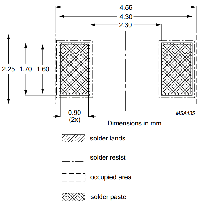
SMT Surface Mount Technology footprint references
http://en.wikipedia.org/wiki/Surface-mount_technology
Surface-mount technology (SMT) is a method for producing electronic circuits in which the components are mounted or placed directly onto the surface of printed circuit boards (PCBs).
An electronic device so made is called a surface-mount device (SMD).
In the industry it has largely replaced the through-hole technology construction method of fitting components with wire leads into holes in the circuit board.
Both technologies can be used on the same board for components not suited to surface mounting such as large transformers and heat-sinked power semiconductors.
An SMT component is usually smaller than its through-hole counterpart because it has either smaller leads or no leads at all. It may have short pins or leads of various styles, flat contacts, a matrix of solder balls (BGAs), or terminations on the body of the component.
Because "surface-mount" refers to a methodology of manufacturing, there are different terms used when referring to the different aspect of the method, which distinguishes for example the components, technique and machines used in manufacturing. These terms are listed in the following table:
| SMp term | Expanded form |
|---|---|
| SMD | Surface-mount devices (active, passive and electromechanical components) |
| SMT | Surface-mount technology (assembling and mounting technology) |
| SMA | Surface-mount assembly (module assembled with SMT) |
| SMC | Surface-mount components (components for SMT) |
| SMP | Surface-mount packages (SMD case forms) |
| SME | Surface-mount equipment (SMT assembling machines) |
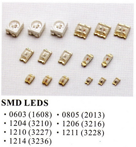
Surface-mount components are usually smaller than their counterparts with leads, and are designed to be handled by machines rather than by humans. The electronics industry has standardized package shapes and sizes (the leading standardisation body is JEDEC). These include:
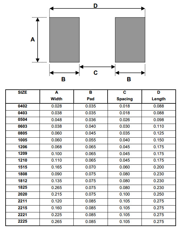
The codes given in the chart below usually tell the length and width of the components in tenths of millimeters or hundredths of inches.
For example, a metric 2520 component is 2.5mm by 2.0mm which corresponds roughly to .10 inches by .08 inches (hence, imperial size is 1008).
Exceptions occur for imperial in the two smallest rectangular passive sizes. The metric codes still represent the dimensions in mm, even though the imperial size codes are no longer aligned.
Problematically, some manufacturers are developing metric 0201 components with dimensions of 0.25 mm × 0.125 mm (0.0098 in × 0.0049 in),[7]
but the imperial 01005 name is already being used for the 0.4 mm × 0.2 mm (0.016 in × 0.0079 in) package.
Example of component sizes, metric and imperial codes and comparison included
- Two-terminal packages
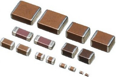
- Rectangular passive components (mostly resistors and capacitors):
- 01005 (0402 metric): 0.4 mm × 0.2 mm (0.016 in × 0.0079 in). Typical power rating for resistors = 0.031 watt[8]
- 0201 (0603 metric): 0.6 mm × 0.3 mm (0.024 in × 0.012 in). Typical power rating for resistors = 0.05 watt[8]
- 0402 (1005 metric): 1.0 mm × 0.5 mm (0.039 in × 0.020 in). Typical power rating for resistors = 0.1 [8]or 0.062 watt[9]
- 0603 (1608 metric): 1.6 mm × 0.8 mm (0.063 in × 0.031 in). Typical power rating for resistors = 0.1 watt[8]
- 0805 (2012 metric): 2.0 mm × 1.25 mm (0.079 in × 0.049 in). Typical power rating for resistors = 0.125 watt[8]
- 1008 (2520 metric): 2.5 mm × 2.0 mm (0.098 in × 0.079 in). Typical inductor and ferrite bead package[10]
- 1206 (3216 metric): 3.2 mm × 1.6 mm (0.13 in × 0.063 in). Typical power rating for resistors = 0.25 watt[8]
- 1210 (3225 metric): 3.2 mm × 2.5 mm (0.13 in × 0.098 in). Typical power rating for resistors = 0.5 watt[8]
- 1806 (4516 metric): 4.5 mm × 1.6 mm (0.18 in × 0.063 in)[11]
- 1812 (4532 metric): 4.5 mm × 3.2 mm (0.18 in × 0.13 in). Typical power rating for resistors = 0.75 watt[8]
- 2010 (5025 metric): 5.0 mm × 2.5 mm (0.20 in × 0.098 in). Typical power rating for resistors = 0.75 watt[8]
- 2512 (6332 metric): 6.4 mm × 3.2 mm (0.25 in × 0.13 in). Typical power rating for resistors = 1 watt[8]
- 2920: 7.4 mm × 5.1 mm (0.29 in × 0.20 in)[12]


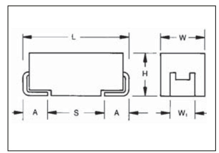
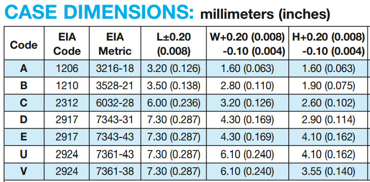
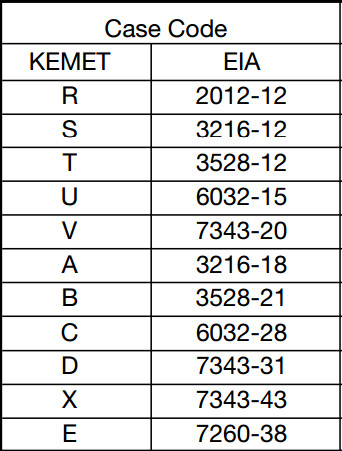
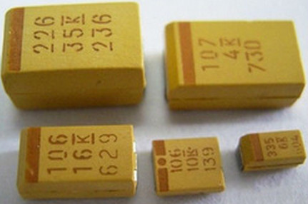
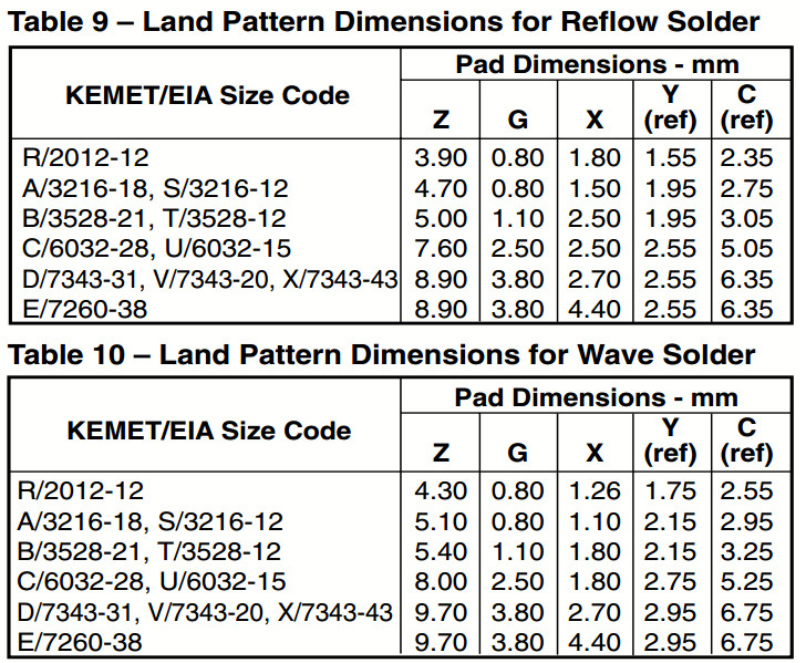
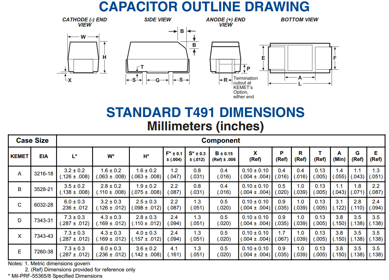
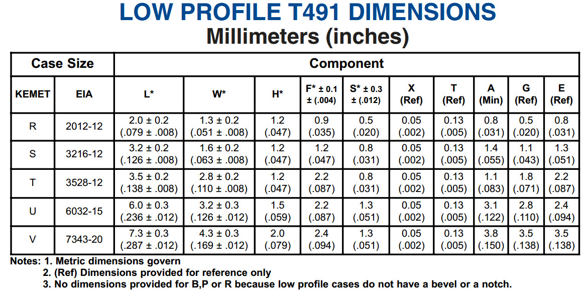
- Tantalum capacitors length (typ.) x width (typ.) x height (max.):[13][14]
- EIA 2012-12 (Kemet R, AVX R): 2.0 mm × 1.3 mm × 1.2 mm
- EIA 3216-10 (Kemet I, AVX K): 3.2 mm × 1.6 mm × 1.0 mm
- EIA 3216-12 (Kemet S, AVX S): 3.2 mm × 1.6 mm × 1.2 mm
- EIA 3216-18 (Kemet A, AVX A): 3.2 mm × 1.6 mm × 1.8 mm
- EIA 3528-12 (Kemet T, AVX T): 3.5 mm × 2.8 mm × 1.2 mm
- EIA 3528-21 (Kemet B, AVX B): 3.5 mm × 2.8 mm × 2.1 mm
- EIA 6032-15 (Kemet U, AVX W): 6.0 mm × 3.2 mm × 1.5 mm
- EIA 6032-28 (Kemet C, AVX C): 6.0 mm × 3.2 mm × 2.8 mm
- EIA 7260-38 (Kemet E, AVX V): 7.3 mm × 6.0 mm × 3.8 mm
- EIA 7343-20 (Kemet V, AVX Y): 7.3 mm × 4.3 mm × 2.0 mm
- EIA 7343-31 (Kemet D, AVX D): 7.3 mm × 4.3 mm × 3.1 mm
- EIA 7343-43 (Kemet X, AVX E): 7.3 mm × 4.3 mm × 4.3 mm
http://www.digikey.com/Web%20Export/Supplier%20Content/Kemet_399/PDF/Kemet_TantalumSMCap.pdf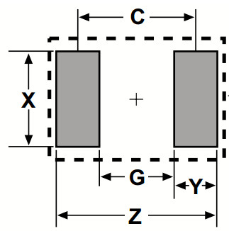
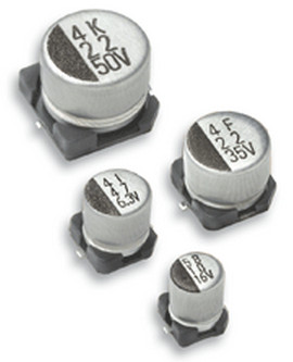
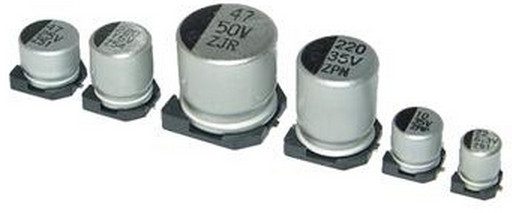
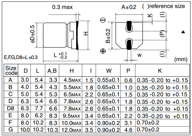
- Aluminium capacitors:[15][16][17]
- (Panasonic A, Chemi-Con B): 3.3 mm × 3.3 mm
- (Panasonic B, Chemi-Con D): 4.3 mm × 4.3 mm
- (Panasonic C, Chemi-Con E): 5.3 mm × 5.3 mm
- (Panasonic D, Chemi-Con F): 6.6 mm × 6.6 mm
- (Panasonic E/F, Chemi-Con H): 8.3 mm × 8.3 mm
- (Panasonic G, Chemi-Con J): 10.3 mm × 10.3 mm
- (Chemi-Con K): 13.0 mm × 13.0 mm
- (Panasonic H): 13.5 mm × 13.5 mm
- (Panasonic J, Chemi-Con L): 17.0 mm × 17.0 mm
- (Panasonic K, Chemi-Con M): 19.0 mm × 19.0 mm
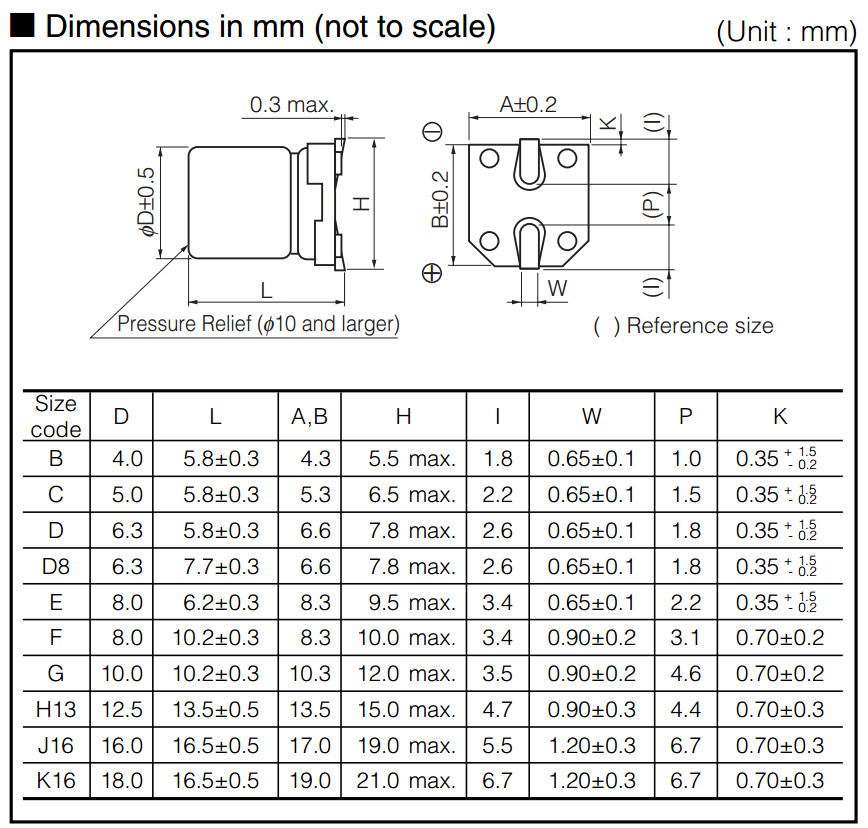
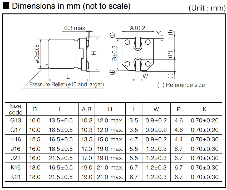
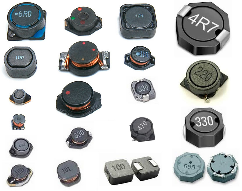
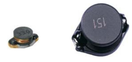
- Power Inductor
- (Panasonic A, Chemi-Con B): 3.3 mm × 3.3 mm
LBS Series SMD Power Inductors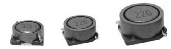
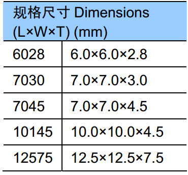
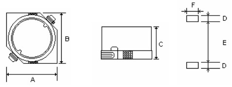
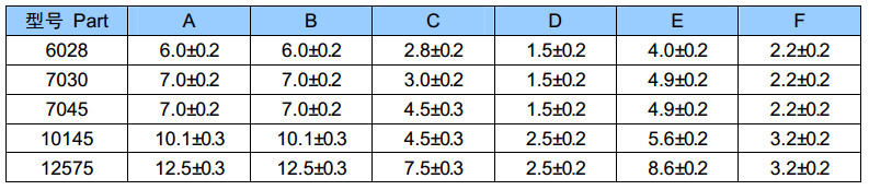
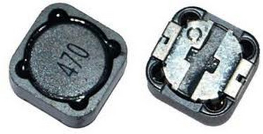
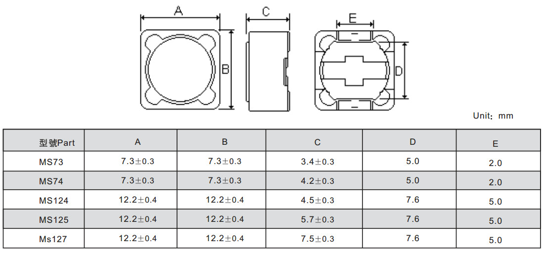
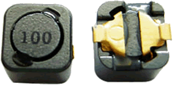
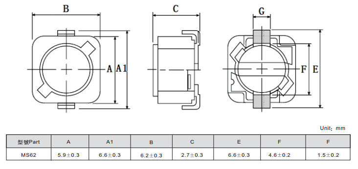
MS Series SMD Power Inductors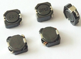
MS103R/104R/105R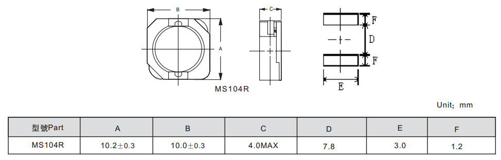
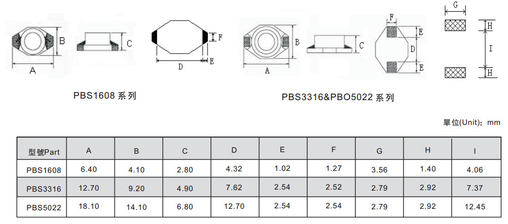
PBS Series SMD Power Inductors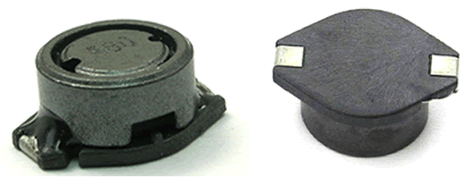
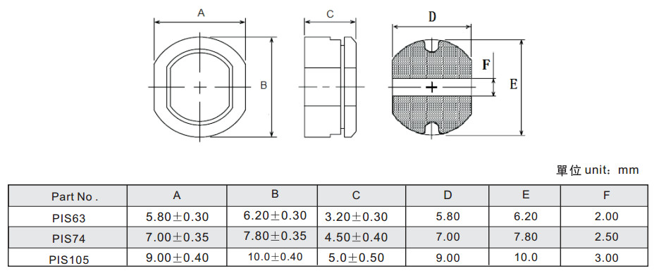
PIS Series SMD Power Inductors
PS-D Series SMD Power Inductors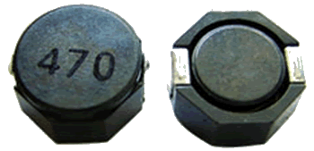
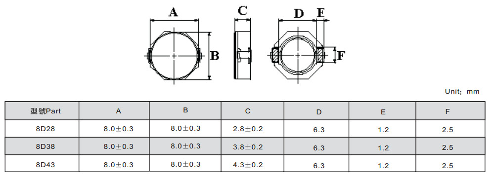
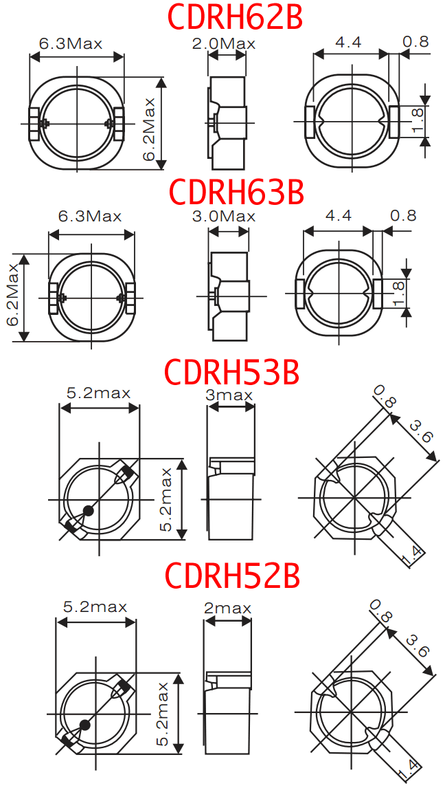

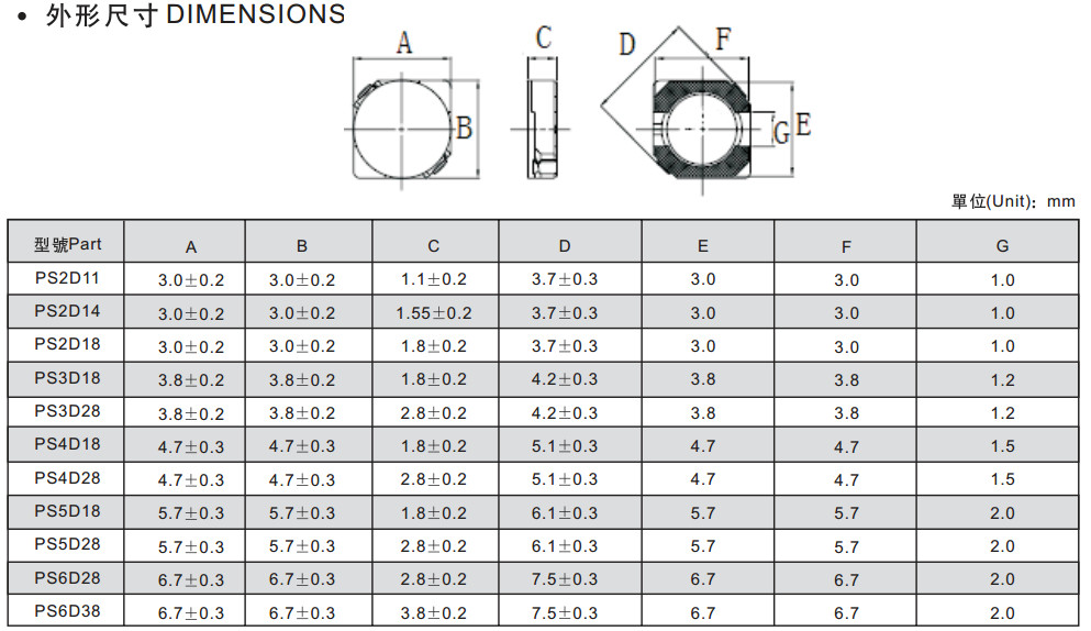
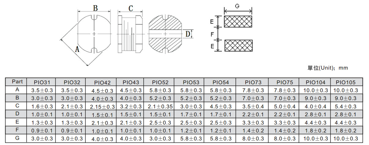
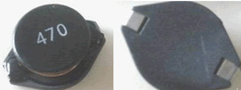
PIO SERIES SMD POWER INDUCTORS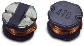
PBO SERIES SMD POWER INDUCTORS
PBO-M SERIES SMD POWER INDUCTORS
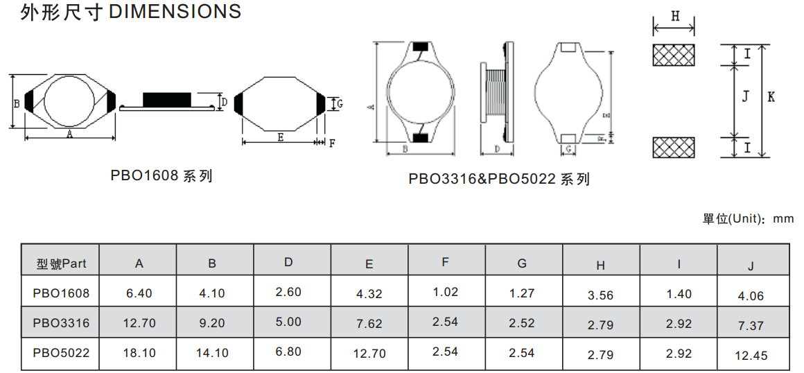
PBO-M SERIES SMD POWER INDUCTORS
- (Panasonic A, Chemi-Con B): 3.3 mm × 3.3 mm
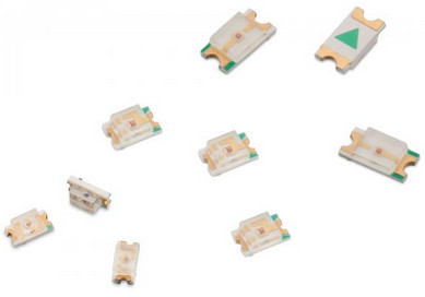
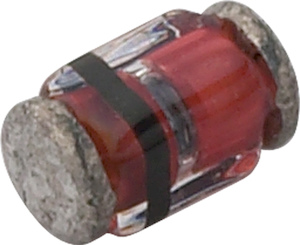
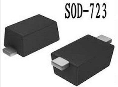
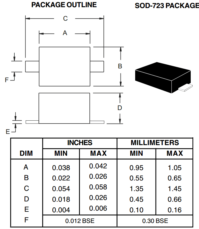
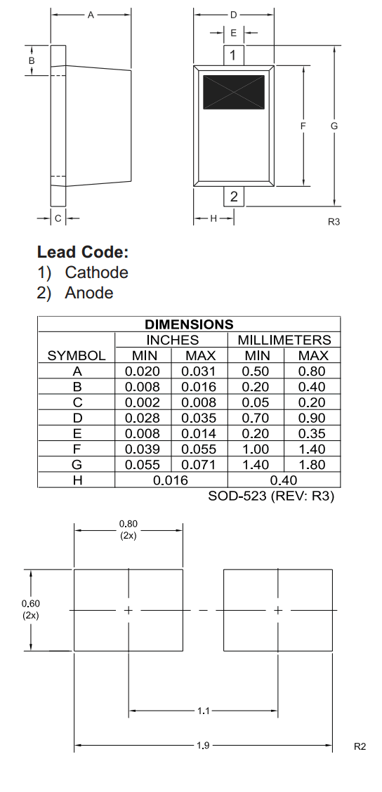
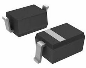
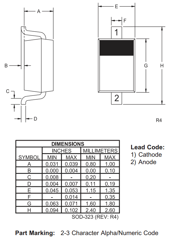
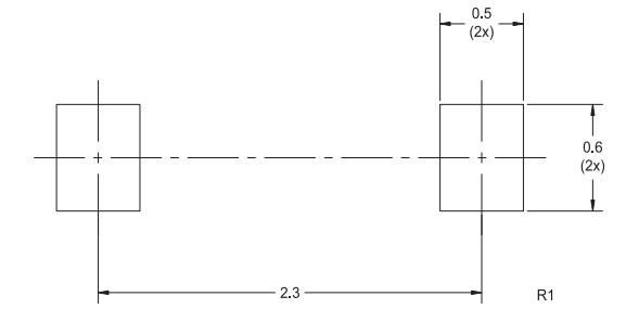
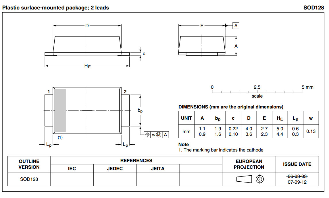
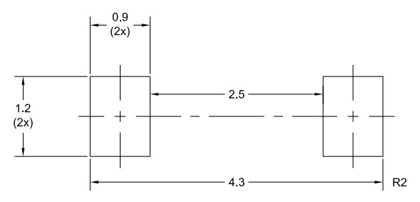
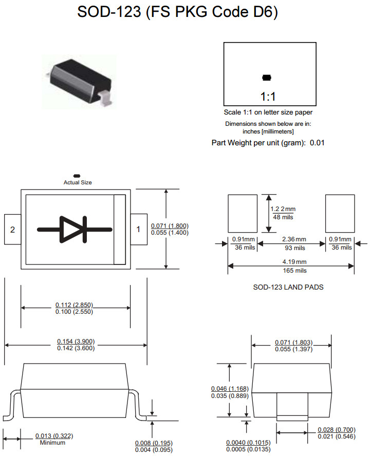
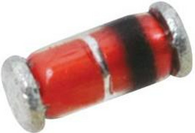
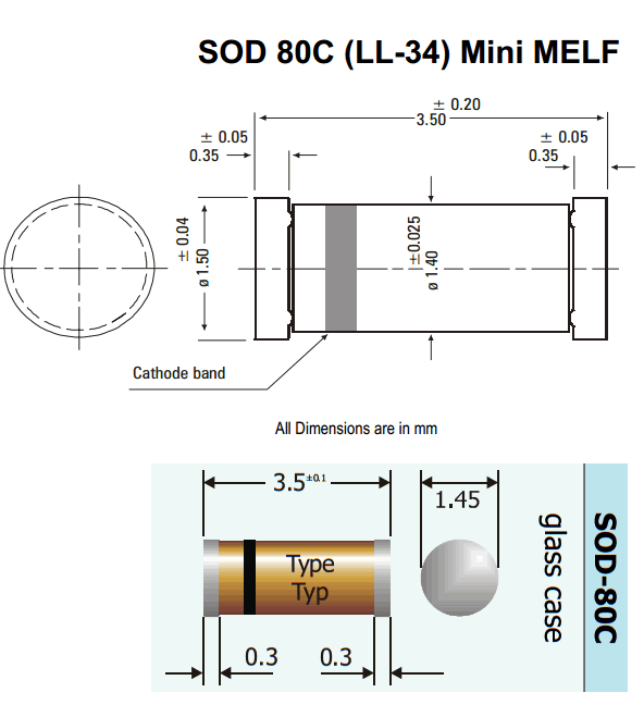
- SOD: Small Outline Diode
http://www.soselectronic.cz/a_info/resource/b/diotec/smd-discretes.pdf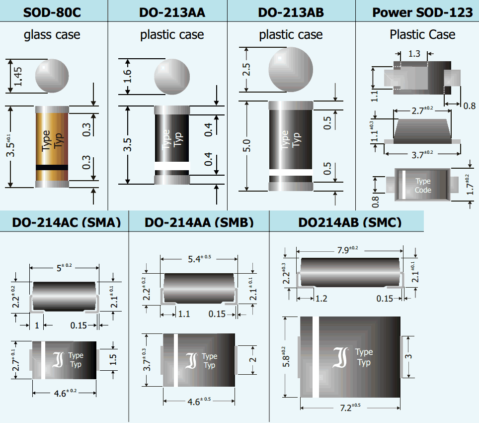
http://www.vishay.com/diodes/
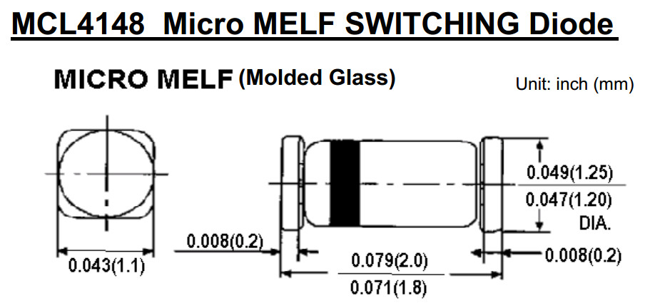
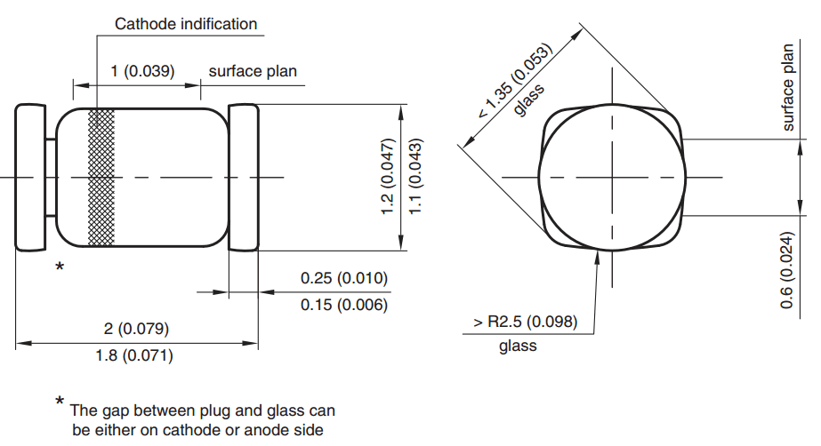
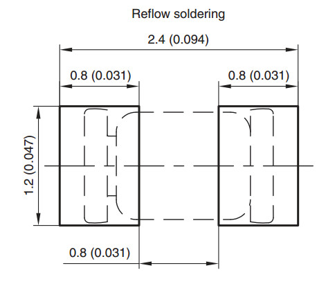
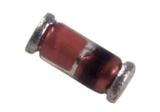
- MELF (Metal Electrode Leadless Face): mostly resistors and diodes; barrel shaped components,
dimensions do not match those of rectangular references for identical codes.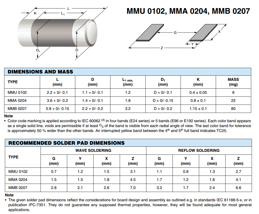
- MicroMelf (MMU) Size 0102: length: 2.2 mm, diam.: 1.1 mm. Typical rating for resistors = 0.2 to 0.3 watt / 150 V[24]
- MiniMelf (MMA) Size 0204: length: 3.6 mm, diam.: :1.4 mm. Typical rating for resistors = 0.25 to 0.4 watt / 200 V[24]

- Melf (MMB) Size 0207: length: 5.8 mm, diam.: 2.2 mm. Typical rating for resistors = 0.4 to 1 watt / 300 V[24]
- MicroMelf (MMU) Size 0102: length: 2.2 mm, diam.: 1.1 mm. Typical rating for resistors = 0.2 to 0.3 watt / 150 V[24]
- Rectangular passive components (mostly resistors and capacitors):
- Three-terminal packages
- SOT: Small Outline Transistor, three terminals
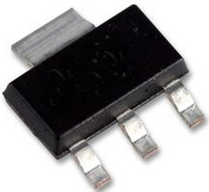
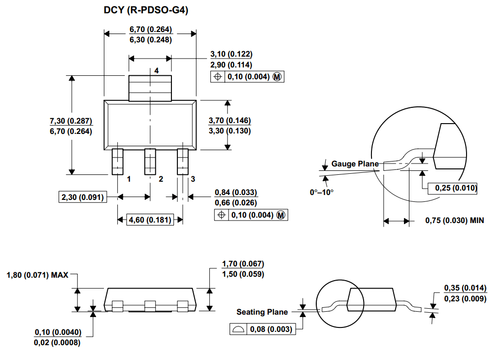
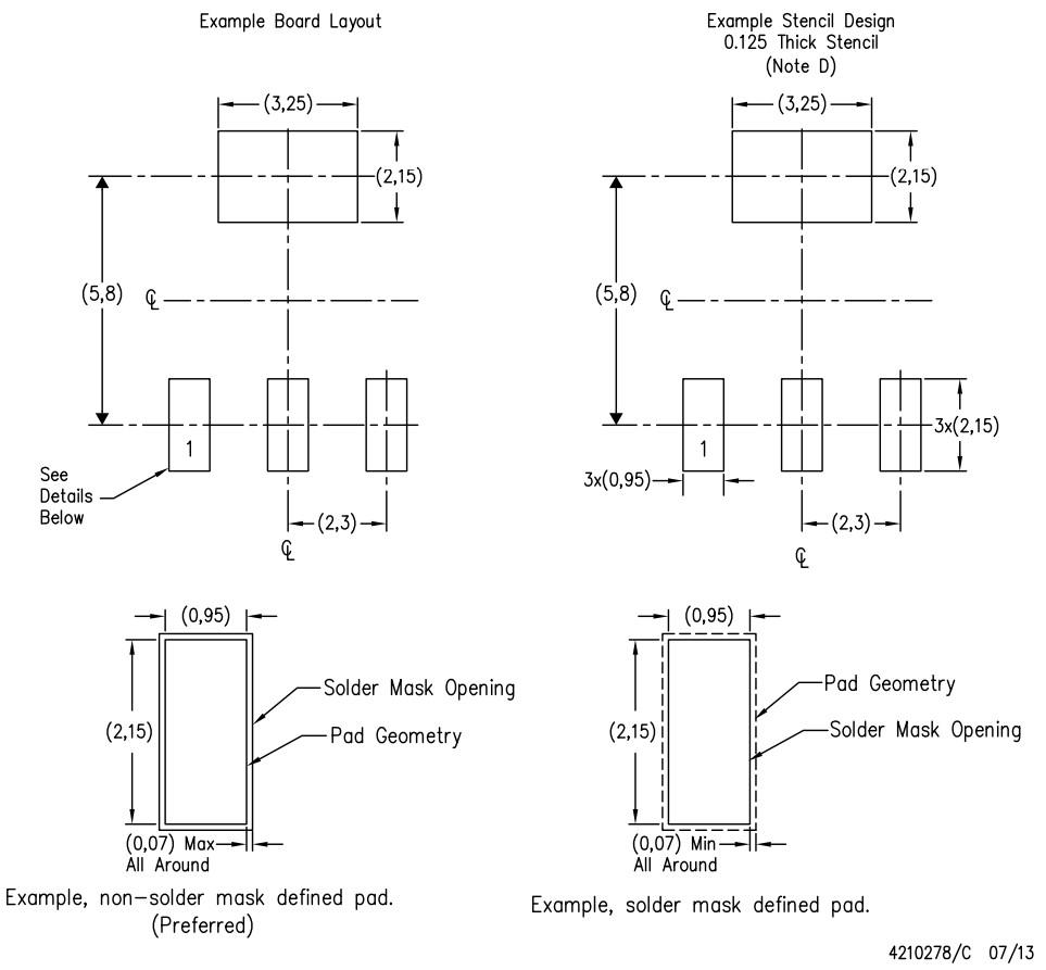
- SOT-223 (SC-73): 6.7 mm × 3.7 mm × 1.8 mm body: four terminals, one of which is a large heat-transfer pad [25]
- SOT-223-6
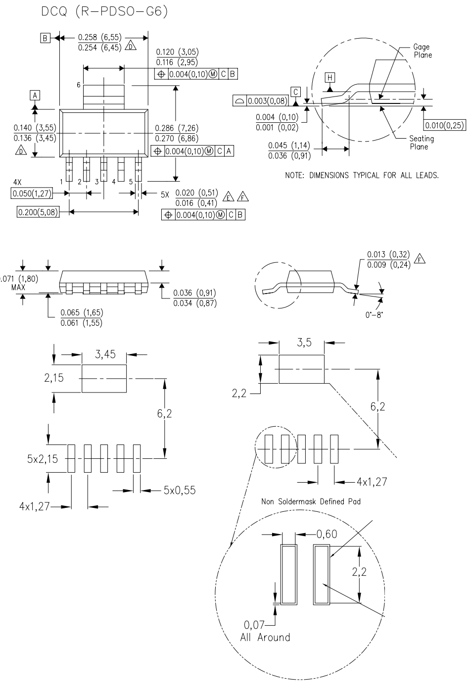
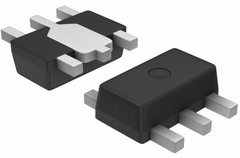
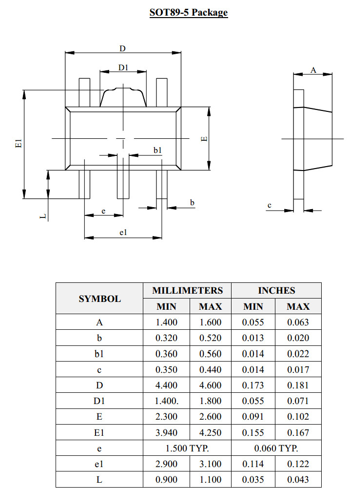
- SOT-89: 4.5 mm × 2.5 mm × 1.5 mm body: four terminals, center pin is connected to a large heat-transfer pad [26]
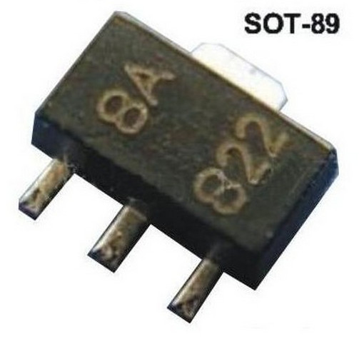
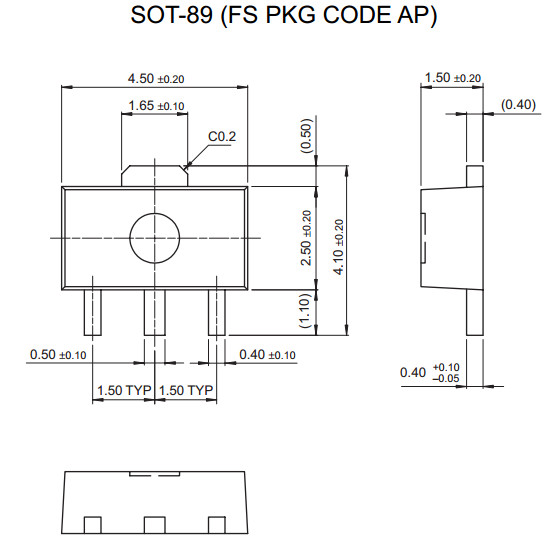
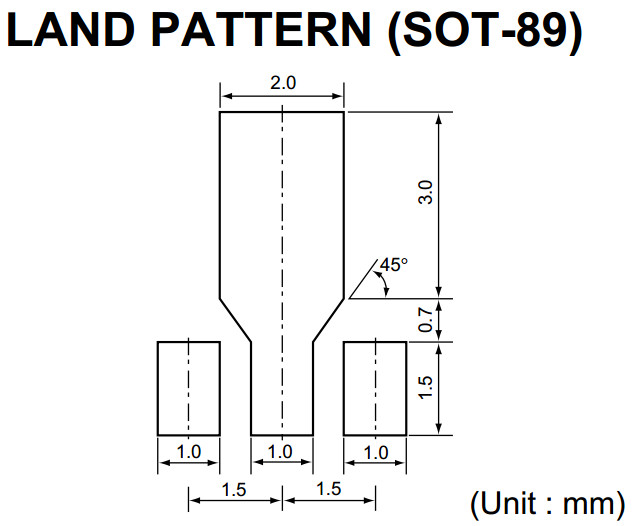
- SOT89-5
- SOT-23 (SC-59, TO-236-3): 2.9 mm × 1.3/1.75 mm × 1.3 mm body: three terminals for a transistor [27]
- SOT-323 (SC-70): 2 mm × 1.25 mm × 0.95 mm body: three terminals [28]
- SOT-416 (SC-75): 1.6 mm × 0.8 mm × 0.8 mm body: three terminals [29]
- SOT-663: 1.6 mm × 1.6 mm × 0.55 mm body: three terminals [30]
- SOT-723: 1.2 mm × 0.8 mm × 0.5 mm body: three terminals: flat lead[31]
- SOT-883 (SC-101): 1 mm × 0.6 mm × 0.5 mm body: three terminals: leadless [32]
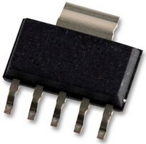
- SOT-223 (SC-73): 6.7 mm × 3.7 mm × 1.8 mm body: four terminals, one of which is a large heat-transfer pad [25]
- DPAK (TO-252, SOT-428): Discrete Packaging.
Developed by Motorola to house higher powered devices. Comes in three- or five-terminal versions [33] - D2PAK (TO-263, SOT-404): bigger than the DPAK;
basically a surface mount equivalent of the TO220 through-hole package.
Comes in 3, 5, 6, 7, 8 or 9-terminal versions [34] - D3PAK (TO-268): even larger than D2PAK [35]
- SOT: Small Outline Transistor, three terminals
- Five- and six-terminal packages
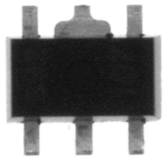
- SOT: small-outline transistor, with more than three terminals
- SOT-23-5 (SOT-25): 2.9 mm × 1.3/1.75 mm × 1.3 mm body: five terminals [36]
- SOT-23-6 (SOT-26): 2.9 mm × 1.3/1.75 mm × 1.3 mm body: six terminals [37]
- SOT-23-8 (SOT-28): 2.9 mm × 1.3/1.75 mm × 1.3 mm body: eight terminals [38]
- SOT-353 (SC-88A): 2 mm × 1.25 mm × 0.95 mm body: five terminals [39]
- SOT-363 (SC-88, SC-70-6): 2 mm × 1.25 mm × 0.95 mm body: six terminals [40]
- SOT-563: 1.6 mm × 1.2 mm × 0.6 mm body: six terminals [41]
- SOT-665: 1.6 mm × 1.6 mm × 0.55 mm body: six terminals [42]
- SOT-666: 1.6 mm × 1.6 mm × 0.55 mm body: six terminals [43]
- SOT-886: 1.5 mm × 1.05 mm × 0.5 mm body: six terminals: leadless
- SOT-886: 1 mm × 1.45 mm × 0.5 mm body: six terminals: leadless [44]
- SOT-891: 1.05 mm × 1.05 mm × 0.5 mm body: five terminals: leadless
- SOT-953: 1 mm × 1 mm × 0.5 mm body: five terminals
- SOT-963: 1 mm × 1 mm × 0.5 mm body: six terminals
- SOT-1115: 0.9 mm × 1 mm × 0.35 mm body: six terminals: leadless [45]
- SOT-1202: 1 mm × 1 mm × 0.35 mm body: six terminals: leadless [46]
- SOT: small-outline transistor, with more than three terminals


- Packages with more than six terminals[47]
- Dual-in-line
- flatpack was one of the earliest surface-mounted packages.
- SOIC: (Small-Outline Integrated Circuit), dual-in-line, 8 or more pins, gull-wing lead form, pin spacing 1.27 mm
- SOJ: Small-Outline Package, J-Leaded, the same as SOIC except J-leaded [48]
- TSOP: Thin Small-Outline Package, thinner than SOIC with smaller pin spacing of 0.5 mm
- SSOP: Shrink Small-Outline Package, pin spacing of 0.65 mm, sometimes 0.635 mm or in some cases 0.8 mm
- TSSOP: Thin Shrink Small-Outline package.
- QSOP: Quarter-Size Small-Outline package, with pin spacing of 0.635 mm
- VSOP: Very Small Outline Package, even smaller than QSOP; 0.4, 0.5 mm or 0.65 mm pin spacing
- DFN: Dual Flat No-lead, smaller footprint than leaded equivalent
- Quad-in-line
- PLCC: Plastic Leaded Chip Carrier, square, J-lead, pin spacing 1.27 mm
- QFP: Quad Flat Package, various sizes, with pins on all four sides
- LQFP: Low-profile Quad Flat Package, 1.4 mm high, varying sized and pins on all four sides
- PQFP: Plastic Quad Flat-Pack, a square with pins on all four sides, 44 or more pins
- CQFP: Ceramic Quad Flat-Pack, similar to PQFP
- MQFP: Metric Quad Flat Pack, a QFP package with metric pin distribution
- TQFP: Thin Quad Flat Pack, a thinner version of PQFP
- QFN: Quad Flat No-lead, smaller footprint than leaded equivalent
- LCC: Leadless Chip Carrier, contacts are recessed vertically to "wick-in" solder. Common in aviation electronics because of robustness to mechanical vibration.
- MLP (MLF): Micro Leadframe Package (Micro Lead-Frame package) with a 0.5 mm contact pitch, no leads (same as QFN) [49]
- PQFN: Power Quad Flat No-lead, with exposed die-pad[s] for heatsinking
- Grid arrays
- PGA: Pin grid array.
- BGA: Ball Grid Array, with a square or rectangular array of solder balls on one surface, ball spacing typically 1.27 mm
- LGA: An array of bare lands only. Similar to in appearance to QFN, but mating is by spring pins within a socket rather than solder.
- FBGA: Fine pitch Ball Grid Array, with a square or rectangular array of solder balls on one surface
- LFBGA: Low profile Fine pitch Ball Grid Array, with a square or rectangular array of solder balls on one surface, ball spacing typically 0.8 mm
- TFBGA: Thin Fine pitch Ball Grid Array, with a square or rectangular array of solder balls on one surface, ball spacing typically 0.5 mm
- CGA: Column Grid Array, circuit package in which the input and output points are high temperature solder cylinders or columns arranged in a grid pattern.
- CCGA: Ceramic Column Grid Array, circuit package in which the input and output points are high temperature solder cylinders or columns arranged in a grid pattern. The body of the component is ceramic.
- μBGA: micro-BGA, with ball spacing less than 1 mm
- LLP: Lead Less Package, a package with metric pin distribution (0.5 mm pitch).
- Non-packaged devices (although surface-mount, these devices require specific process for assembly):
- COB: Chip-On-Board; a bare silicon chip, that is usually an integrated circuit,
is supplied without a package (usually a lead frame overmolded with epoxy)
and is attached, often with epoxy, directly to a circuit board.
The chip is then wire bonded and protected from mechanical
damage and contamination by an epoxy "glob-top". - COF: Chip-On-Flex; a variation of COB, where a chip is mounted directly to a flex circuit.
- COG: Chip-On-Glass; a variation of COB, where a chip,
typically a Liquid crystal display (LCD) controller, is mounted directly on glass.
- COB: Chip-On-Board; a bare silicon chip, that is usually an integrated circuit,
- Dual-in-line

