74HC245 74HCT245 74LV245 74LVC245 74LVC4245A 74LVC8T245 74LVC16T245 74ALVC164245
74HC245/74HCT245
The 74HC245; 74HCT245 is a high-speed Si-gate CMOS device and is
pin compatible with Low-Power Schottky TTL (LSTTL).
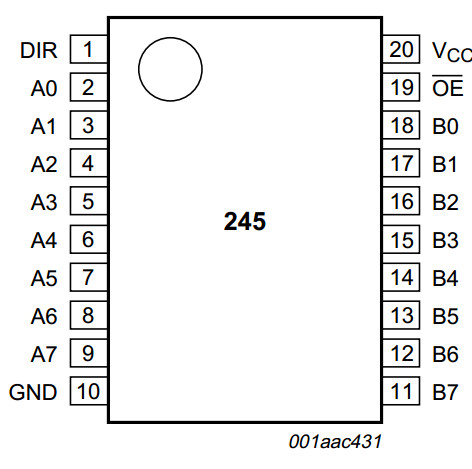
The 74HC245; 74HCT245 is an octal transceiver featuring non-inverting 3-state bus
compatible outputs in both send and receive directions.
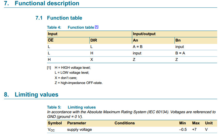
The 74HC245; 74HCT245 features an output enable input (OE) for easy cascading
and a send/receive input (DIR) for direction control.
OE controls the outputs so that the buses are effectively isolated.
The 74HC245; 74HCT245 is similar to the 74HC640;
74HCT640 but has true (non-inverting) outputs.
■ Octal bidirectional bus interface
■ Non-inverting 3-state outputs
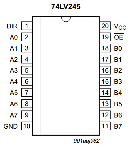
74LV245
Octal bus transceiver (3-State)
The 74LV245 is a low-voltage Si-gate CMOS device that is pin
and function compatible with 74HC245 and 74HCT245.
The 74LV245 is an octal transceiver with non-inverting 3-state bus
compatible outputs in both send and receive directions.
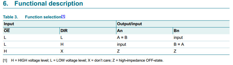
A send/receive (DIR) input controls direction, and an output enable (OE)
input makes easy cascading possible.
Pin OE controls the outputs so that the buses are effectively isolated.
Wide operating voltage: 1.0 V to 5.5 V
Optimized for low voltage applications: 1.0 V to 3.6 V
Accepts TTL input levels between VCC = 2.7 V and VCC = 3.6 V
Typical output ground bounce < 0.8 V at VCC = 3.3 V and Tamb = 25 °C
Typical HIGH-level output voltage (VOH) undershoot: > 2 V at VCC = 3.3 V and Tamb = 25 °C
74LV245A
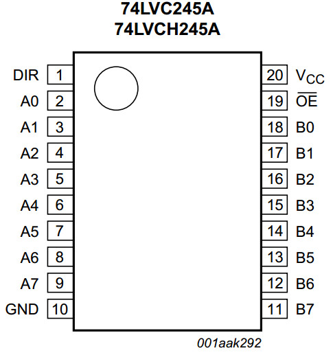
The 74LVC245A; 74LVCH245A are 8-bit transceivers featuring non-inverting 3-state bus
compatible outputs in both send and receive directions.
The device features an output enable (OE) input for easy cascading and
a send/receive (DIR) input for direction control.
OE controls the outputs so that the buses are effectively isolated.
Inputs can be driven from either 3.3 V or 5 V devices.
When disabled, up to 5.5 V can be applied to the outputs.
These features allow the use of these devices in mixed 3.3 V and 5 V applications.
The 74LVCH245A bus hold on data inputs eliminates the need for external pull-up
resistors to hold unused inputs.
5 V tolerant inputs/outputs for interfacing with 5 V logic
Wide supply voltage range from 1.2 V to 3.6 V
74LVC4245A
Octal dual supply translating transceiver; 3-state
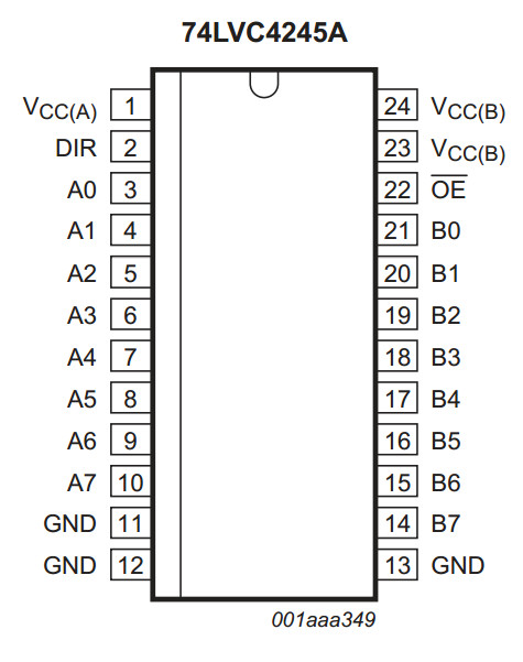
The 74LVC4245A is an octal dual supply translating transceiver featuring
non-inverting 3-state bus compatible outputs in both send and receive directions.
It is designed to interface between a 3 V and 5 V bus
in a mixed 3 V and 5 V supply environment.
The device features an output enable input (pin OE) for
easy cascading and a send/receive input (pin DIR) for direction control.
Pin OE controls the outputs so that the buses are effectively isolated.
In suspend mode, when VCC(A) is zero, there will be
no current flow from one supply to the other supply.
The A-outputs must be set 3-state and the voltage on the A-bus
must be smaller than Vdiode (typical 0.7 V).
VCC(A) >= VCC(B), except in suspend mode.
5 V tolerant inputs/outputs, for interfacing with 5 V logic
Wide supply voltage range:
3 V bus (VCC(B)): 1.5 V to 3.6 V
5 V bus (VCC(A)): 1.5 V to 5.5 V
CMOS low-power consumption
Direct interface with TTL levels
Inputs accept voltages up to 5.5 V
High-impedance when VCC(A) = 0 V
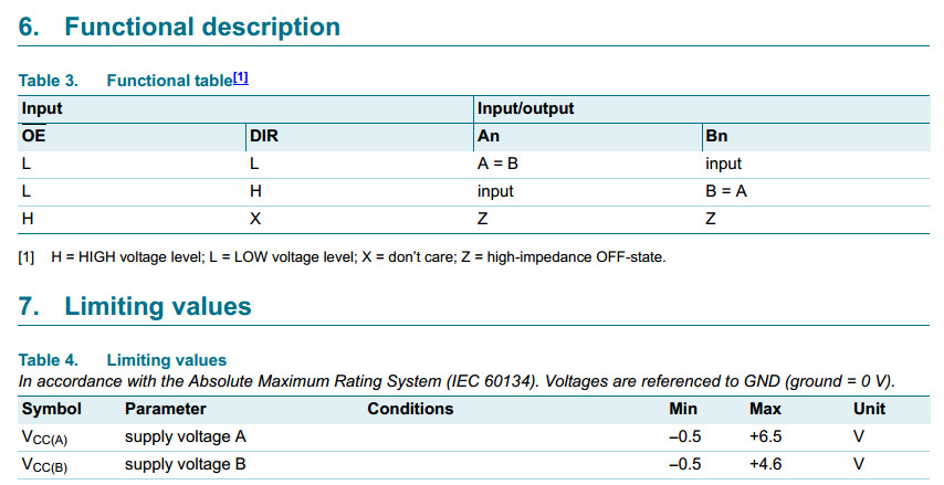
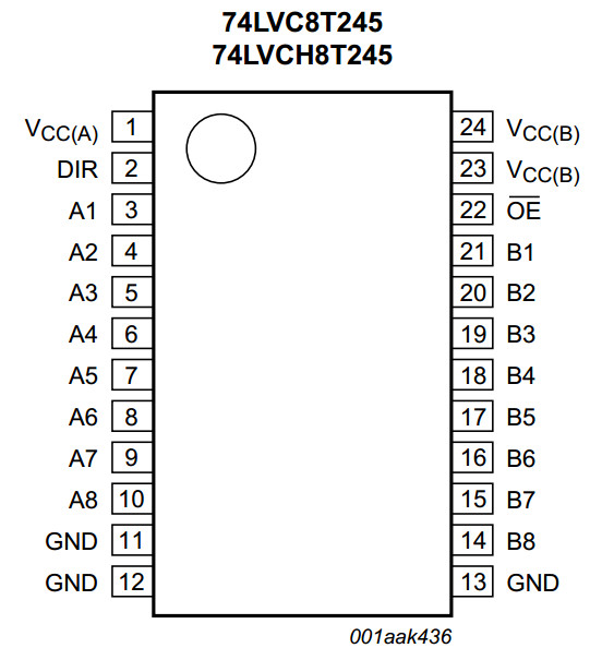
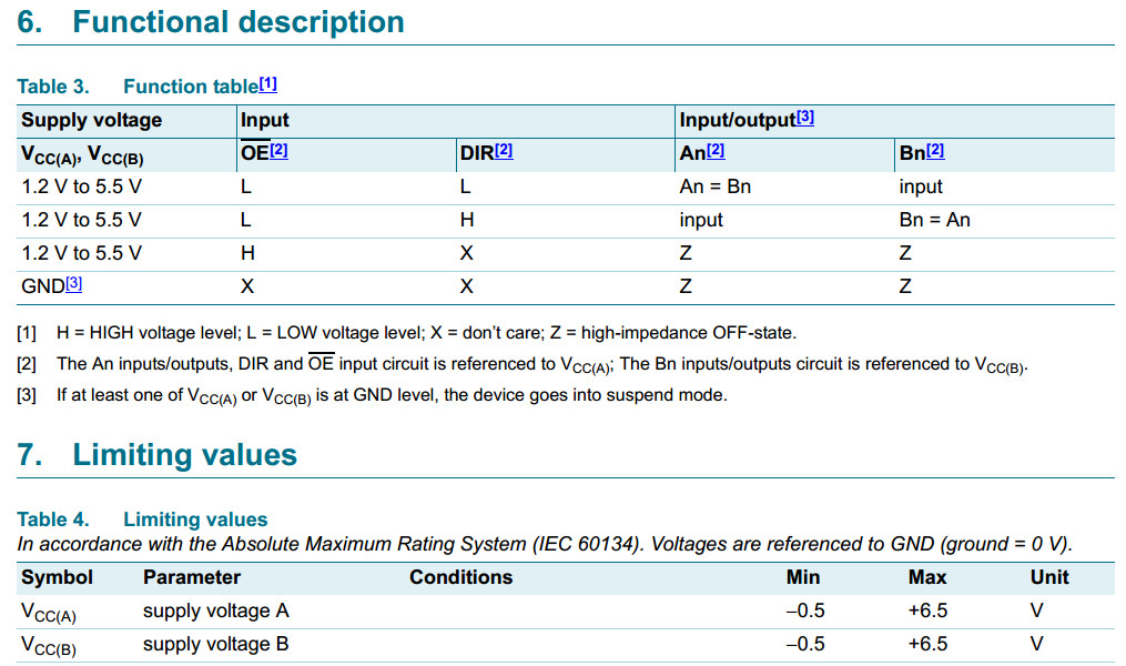
74LVC8T245
The 74LVC8T245; 74LVCH8T245 are 8-bit dual supply translating transceivers
with 3-state outputs that enable bidirectional level translation.
They feature two data input-output ports (pins An and Bn), a direction control input (DIR),
an output enable input (OE) and dual supply pins (VCC(A) and VCC(B)).
Both VCC(A) and VCC(B) can be supplied at any voltage between 1.2 V and 5.5 V
making the device suitable for translating between any of the low voltage nodes
(1.2 V, 1.5 V, 1.8 V, 2.5 V, 3.3 V and 5.0 V).
Pins An, OE and DIR are referenced to VCC(A) and pins Bn are referenced to VCC(B).
A HIGH on DIR allows transmission from An to Bn and
a LOW on DIR allows transmission from Bn to An.
The output enable input (OE) can be used to disable the outputs
so the buses are effectively isolated.
The devices are fully specified for partial power-down applications using IOFF.
The IOFF circuitry disables the output, preventing any damaging backflow current
through the device when it is powered down.
In suspend mode when either VCC(A) or VCC(B) are at GND level,
both A port and B port are in the high-impedance OFF-state.
Active bus hold circuitry in the 74LVCH8T245 holds unused or
floating data inputs at a valid logic level.
Wide supply voltage range:
VCC(A): 1.2 V to 5.5 V
VCC(B): 1.2 V to 5.5 V
74LVC16T245
- Control Inputs VIH/VIL Levels Are Referenced to VCCA Voltage
- VCC Isolation Feature - If Either VCC Input Is at GND,
Both Ports Are in the High-Impedance State - Overvoltage-Tolerant Inputs/Outputs Allow Mixed-Voltage-Mode Data Communications
- Fully Configurable Dual-Rail Design Allows Each Port
to Operate Over the Full 1.65-V to 5.5-V Power-Supply Range
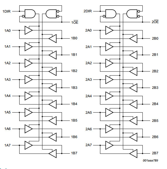
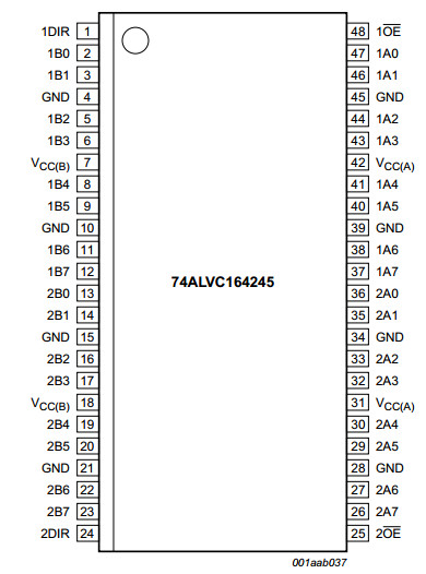
74ALVC164245
16-bit dual supply translating transceiver; 3-state
The 74ALVC164245 is a high-performance, low-power, low-voltage, Si-gate CMOS
device, superior to most advanced CMOS compatible TTL families.
The 74ALVC164245 is a 16-bit (dual octal) dual supply translating transceiver featuring
non-inverting 3-state bus compatible outputs in both send and receive directions. It is
designed to interface between a 3 V and 5 V bus in a mixed 3 V and 5 V supply
environment.
This device can be used as two 8-bit transceivers or one 16-bit transceiver.
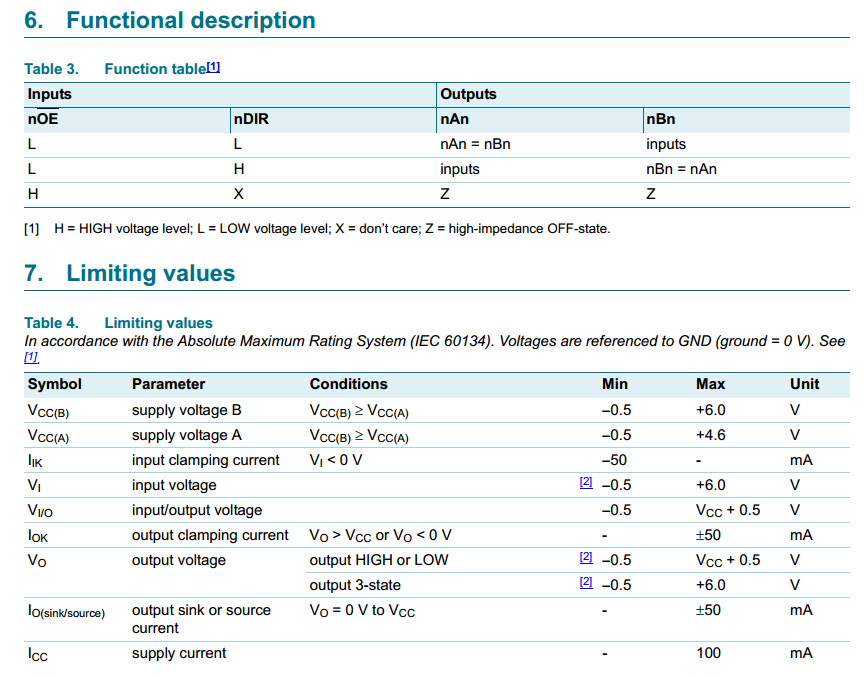
The direction control inputs (1DIR and 2DIR) determine the direction of the data flow.
nDIR (active HIGH) enables data from nAn ports to nBn ports. nDIR (active LOW) enables
data from nBn ports to nAn ports. The output enable inputs (1OE and 2OE), when HIGH,
disable both nAn and nBn ports by placing them in a high-impedance OFF-state. Pins
nAn, nOE and nDIR are referenced to VCC(A) and pins nBn are referenced to VCC(B).
In suspend mode, when one of the supply voltages is zero, there will be no current flow
from the non-zero supply towards the zero supply. The nAn-outputs must be set 3-state
and the voltage on the A-bus must be smaller than Vdiode (typical 0.7 V). VCC(B) VCC(A)
(except in suspend mode).
5 V tolerant inputs/outputs for interfacing with 5 V logic
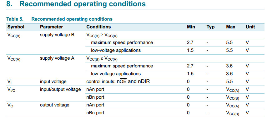
Wide supply voltage range:
3 V port (VCC(A)): 1.5 V to 3.6 V
5 V port (VCC(B)): 1.5 V to 5.5 V
CMOS low power consumption
Direct interface with TTL levels
Control inputs voltage range from 2.7 V to 5.5 V
Inputs accept voltages up to 5.5 V
High-impedance outputs when VCC(A) or VCC(B) = 0 V